Liquid crystal display panel
A liquid crystal display panel and liquid crystal layer technology, applied in static indicators, nonlinear optics, instruments, etc., can solve the problems of color change, low aperture ratio and transmittance, and achieve the effect of good display characteristics
- Summary
- Abstract
- Description
- Claims
- Application Information
AI Technical Summary
Problems solved by technology
Method used
Image

Examples
Embodiment 1
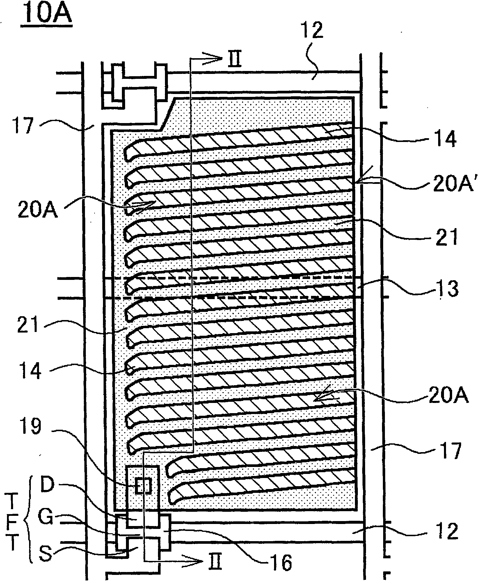
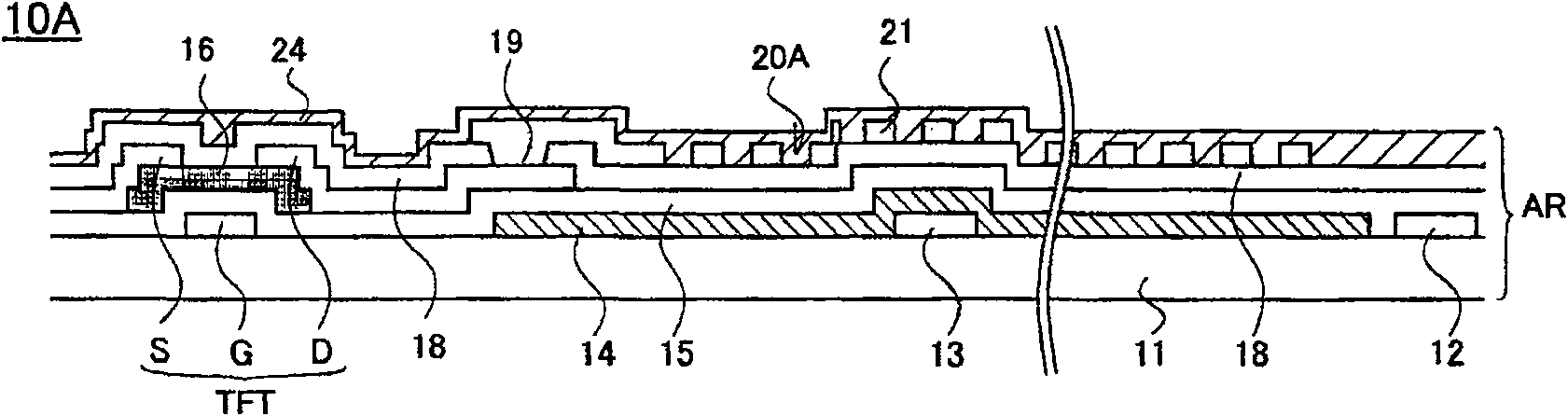
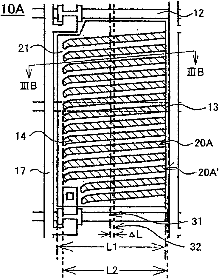
[0093] The liquid crystal display panel of embodiment 1 has: array substrate, and this array substrate has common electrode, the insulating film that is formed on the common electrode, the pixel electrode that is formed on the insulating film; There is the color filter substrate of color filter layer; The liquid crystal layer sandwiched by the color filter substrate; the liquid crystal display panel drives the liquid crystal layer through the electric field generated between the common electrode and the pixel electrode, which is also called the so-called FFS mode liquid crystal display panel. use figure 1 The manufacturing flow of the FFS mode liquid crystal display panel 10A of the first embodiment will be described with reference to FIG. 3 . in, figure 1 It is a schematic plan view showing transparently one pixel of the color filter substrate and the alignment film of the FFS mode liquid crystal display panel of Example 1, figure 2 is along figure 1 Sectional view of ...
Embodiment 2
[0107] Then use Figure 4 The FFS mode liquid crystal display panel 10B of the second embodiment will be described. in, Figure 4 It is a schematic plan view showing transparently one pixel of the color filter substrate and alignment film of the FFS mode liquid crystal display panel of Example 2. and, Figure 4 neutralize figure 1 as well as figure 2 Portions of the FFS mode liquid crystal display panel 10A of the illustrated embodiment 1 having the same structure are given the same reference numerals, and detailed description thereof is omitted.
[0108] The difference in structure between the FFS mode liquid crystal display panel 10B of the second embodiment and the liquid crystal display panel 10A of the first embodiment is that the plurality of slits 20B arranged on the pixel electrodes 21 are arranged on the adjacent scanning lines 12 relative to each other. For the common wiring 13 between them, it is arranged in a state of inclination in different directions in a...
Embodiment 3
[0114] use below Figure 5 The FFS mode liquid crystal display panel 10C of the third embodiment will be described. in, Figure 5 It is a schematic plan view showing transparently some pixels of the color filter substrate and the alignment film of the FFS mode liquid crystal display panel of Example 3. And, for Figure 5 neutralize figure 2 and figure 2 Portions of the FFS mode liquid crystal display panel 10A shown in Embodiment 1 having the same structure are given the same reference numerals, and a detailed description thereof is omitted.
[0115] The difference in structure between the FFS mode liquid crystal display panel 10C of the third embodiment and the liquid crystal display panel 10A of the first embodiment is that each pixel is arranged in a triangle in a different manner on each row, and each pixel A plurality of slits 20C are inclined in opposite directions to each other on the odd-numbered rows and the even-numbered rows, and its other structure is the sa...
PUM
 Abstract
Description
Claims
Application Information
 - R&D
- Intellectual Property
- Life Sciences
- Materials
- Tech Scout
- Unparalleled Data Quality
- Higher Quality Content
- 60% Fewer Hallucinations
Browse by: Latest US Patents, China's latest patents, Technical Efficacy Thesaurus, Application Domain, Technology Topic, Popular Technical Reports.
© 2025 PatSnap. All rights reserved.Legal|Privacy policy|Modern Slavery Act Transparency Statement|Sitemap|About US| Contact US: help@patsnap.com