Solid camera device and camera
A technology of a solid-state imaging device and imaging unit, which is applied in solid-state image signal generators, image communications, and televisions, and can solve problems such as image quality degradation and color mixing
- Summary
- Abstract
- Description
- Claims
- Application Information
AI Technical Summary
Problems solved by technology
Method used
Image
Examples
Embodiment approach 1
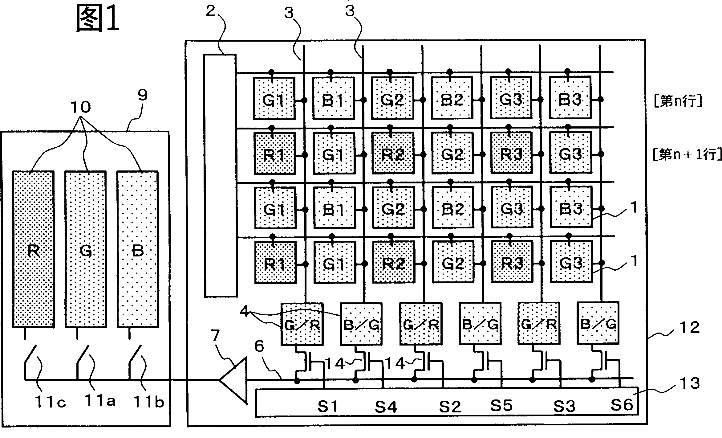
[0034] FIG. 1 is a diagram showing configurations of a MOS solid-state imaging device 12 and an external circuit 9 in Embodiment 1 of the present invention. The same parts as those of the conventional device shown in FIG. 7 are denoted by the same reference numerals, and repeated explanations are omitted.
[0035] The structure of this solid-state imaging device 12 that is different from the conventional example shown in FIG. 7 is the horizontal shift register 13, and other parts are the same as those of the conventional example shown in FIG. 7 . The configuration of the external circuit 9 is also the same as that of the conventional example shown in FIG. 7 . In the pixel 1 of 12 in the solid-state imaging device, red (R), green (G), and blue (B) three primary color pixels 1 are arranged two-dimensionally, and the structure is the same as the conventional example. The horizontal shift register 13 of this embodiment differs from the conventional example in that when the image ...
Embodiment approach 2
[0043] FIG. 3 shows configurations of a MOS solid-state imaging device 15 and an external circuit 17 in Embodiment 2 of the present invention. The same parts as those of the conventional device shown in FIG. 7 are denoted by the same reference numerals, and repeated explanations are omitted.
[0044] The structure of this solid-state imaging device 15 is different from the conventional device shown in FIG. 7 in that it has two output signal lines 6a, 6b. Output amplifiers 7a, 7b are connected to the output signal lines 6a, 6b, respectively. Read switches 16a, 16b are interposed between the line memory section 4 and the output signal lines 6a, 6b. In addition, to the external circuit 17, the color selection switches 11a to 11c are connected according to the division corresponding to the output signals of the output amplifiers 7a and 7b.
[0045] In the pixel 1, the three primary colors of red (R), green (G), and blue (B) are arranged two-dimensionally as in the conventional e...
Embodiment approach 3
[0056] FIG. 5 is a diagram showing configurations of a MOS solid-state imaging device 18 and an external circuit 17 in Embodiment 3 of the present invention. The same parts as those of the conventional device shown in FIG. 7 are denoted by the same reference numerals, and repeated explanations are omitted.
[0057] The structure of this solid-state imaging device 18 is different from the conventional device shown in FIG. 7 in that it has two output signal lines 6a, 6b. Output amplifiers 7a, 7b are connected to the output signal lines 6a, 6b, respectively. Read switches 20a, 20b are interposed between the line memory section 4 and the output signal lines 6a, 6b. In addition, memory selection switches 19 a and 19 b are interposed between the vertical signal line 3 and the row memory section 4 . Each vertical signal line 3 is connected to a storage position (G) or a storage position (B / R) in the line memory section 4 so as to be switched by the memory selection switches 19 a an...
PUM
 Abstract
Description
Claims
Application Information
 - Generate Ideas
- Intellectual Property
- Life Sciences
- Materials
- Tech Scout
- Unparalleled Data Quality
- Higher Quality Content
- 60% Fewer Hallucinations
Browse by: Latest US Patents, China's latest patents, Technical Efficacy Thesaurus, Application Domain, Technology Topic, Popular Technical Reports.
© 2025 PatSnap. All rights reserved.Legal|Privacy policy|Modern Slavery Act Transparency Statement|Sitemap|About US| Contact US: help@patsnap.com


