Navigation method in semiconductor chip conducting wire mending course

A navigation method and semiconductor technology, which are applied in the fields of semiconductor/solid-state device manufacturing, semiconductor/solid-state device testing/measurement, electrical components, etc., can solve the problems of long navigation time, increased cost, low resolution, etc., and achieve short X-ray wavelengths. , the effect of improving the success rate and improving the resolution

Inactive Publication Date: 2009-07-22
SEMICON MFG INT (SHANGHAI) CORP +1
View PDF3 Cites 0 Cited by
  • Summary
  • Abstract
  • Description
  • Claims
  • Application Information

AI Technical Summary

Problems solved by technology

[0007] In the prior art, when the focused ion beam repairs wrong wires on the semiconductor substrate, an infrared microscope is used to navigate to determine the position of the wire layer. Due to the long wavelength of the infrared microscope, the resolution is low, which makes the navigation time long and the accuracy of determining the position of the wire layer Low, which in turn leads to higher costs and lower success rates for repairing wires

Method used


Image

  • Navigation method in semiconductor chip conducting wire mending course
  • Navigation method in semiconductor chip conducting wire mending course
  • Navigation method in semiconductor chip conducting wire mending course

Examples


Embodiment Construction

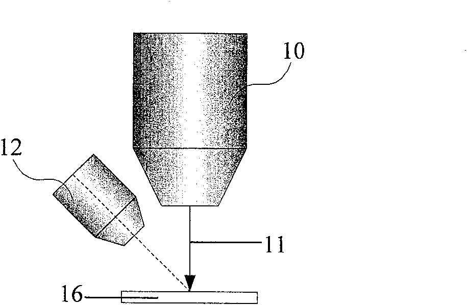
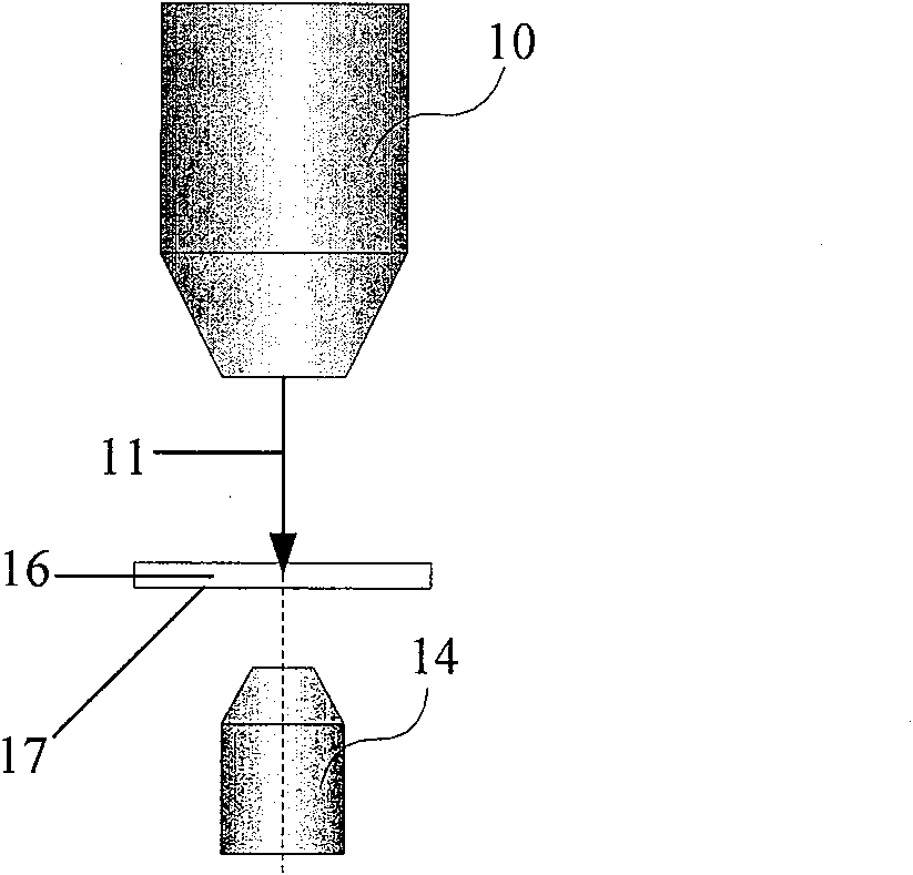
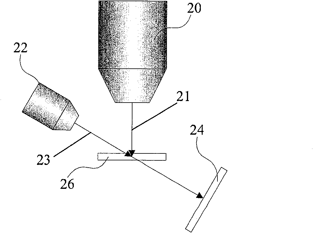
[0021] In recent years, semiconductor integrated circuits have become highly integrated and have more functions. When developing a large-scale integrated circuit, it is necessary to ensure that the wiring is correct. Therefore, when the circuit fails due to wiring errors, focused ion beam processing is required. to fix faulty wires. But because the focused ion beam can see the distance is not deep, so when the focused ion beam is repairing the wire, the navigation system needs to observe in advance. In the prior art, before the focused ion beam repairs the wires on the semiconductor substrate, an infrared microscope is used to navigate and determine the position of the layer line layer. Due to the long wavelength of the infrared microscope, the resolution is low, the navigation time is long, the accuracy is low, and the cost is increased. Increased, the success rate of repairing wires is reduced. The present invention uses an X-ray device to determine the position of the wire...


PUM


Abstract

A navigation method in the process of repairing semiconductor chip conducting wire comprises the following procedures than: a X-ray device and a semiconductor chip are arranged to form an angle, wherein, the X-ray device comprises a X-ray emitter and a X-ray detector; the semiconductor chip comprises a conductor layer; the X-ray emitter emits X-rays which penetrate the semiconductor chip to the X-ray detector; the position of the conductor layer of the semiconductor chip is determined; the conductor layer is scanned; the erroneous conducting wires are found and repaired. Through the procedures, before repairing the erroneous conducting wires of the semiconductor wires by focused ion beams, the position of the conductor layer is determined by the X-ray device; as the X-ray has short wavelength, the resolution factor is improved, thereby improving the accuracy to determine the position of the conductor layer, shortening the navigation time, further achieving the increase of the success rate of repairing the conducting wires and reducing the cost.

Description

technical field [0001] The invention relates to a method for repairing wires on a semiconductor chip by using a focused ion beam, in particular to a method for navigating with an X-ray device when the wires on a semiconductor chip are repaired by a focused ion beam. Background technique [0002] As a means of exposure, focused ion beam has very high sensitivity, mainly because the energy transfer efficiency of ions in solid materials is much higher than that of electrons, and the sensitivity of commonly used electron beam exposure resists to ions is higher than that of The electron beam is more than 100 times higher. Moreover, focused ion beam exposure has almost no proximity effect. Since the mass of the ion itself is much larger than that of the electron, the scattering range of the ion in the resist is much smaller than that of the electron, and there is almost no scattering effect. In addition to the already mentioned extremely high exposure sensitivity and no proximity...

Claims


Application Information

Patent Timeline
Patent Type & Authority Patents(China)
IPC IPC(8): H01L21/768H01L21/66
Inventor 董伟淳季春葵廖炳隆牛崇实
Owner SEMICON MFG INT (SHANGHAI) CORP
Why Eureka
Try Eureka