Optically pumped semiconductor device

A semiconductor and optical pumping technology, applied in semiconductor laser excitation devices, semiconductor lasers, excitation methods/devices, etc., can solve the problems of reduced pumping efficiency, achieve low technical costs, eliminate consistency, and high pumping efficiency Effect

Inactive Publication Date: 2009-03-18
OSRAM OPTO SEMICONDUCTORS GMBH & CO OHG
View PDF5 Cites 0 Cited by
  • Summary
  • Abstract
  • Description
  • Claims
  • Application Information

AI Technical Summary

Problems solved by technology

In addition, there is the risk that the optical properties of the semiconductor body are affected due to the intensive mixing of the quantum wells in the laterally outer region, which leads to a reduction in the pumping efficiency

Method used


Image

  • Optically pumped semiconductor device
  • Optically pumped semiconductor device
  • Optically pumped semiconductor device

Examples


Embodiment Construction

[0037] Identical or identically acting elements are provided with the same reference symbols in these figures.

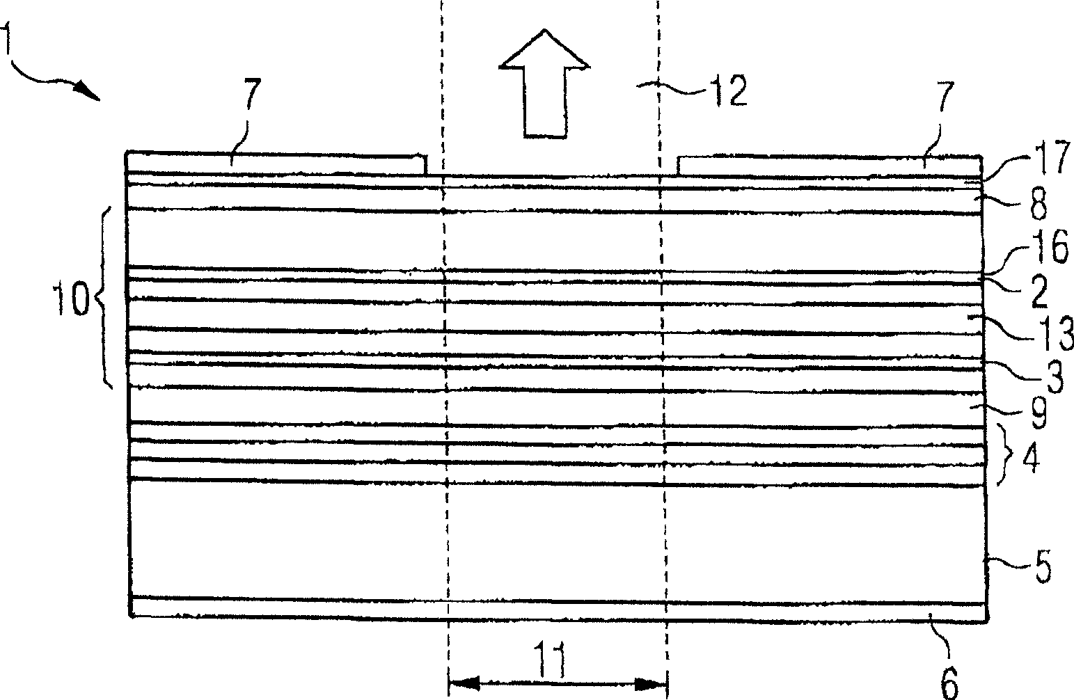
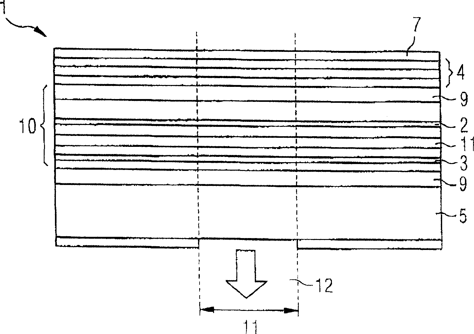
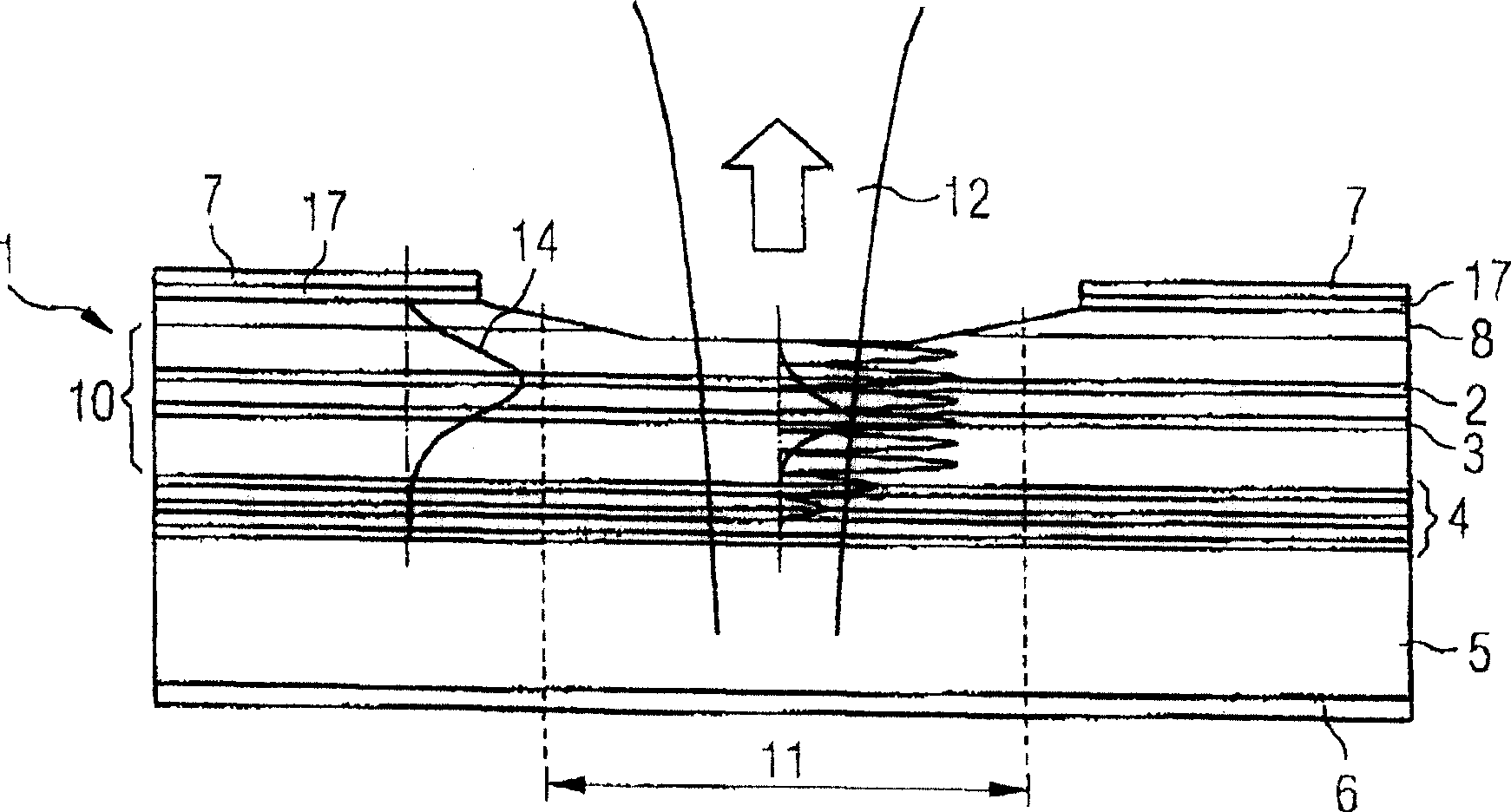
[0038] figure 1 The embodiment of an optically pumped semiconductor device according to the invention shown in has a semiconductor body 1 comprising an active pumping layer 2 and a An active vertical emission layer 3, wherein the pumping layer 2 and the vertical emission layer 3 are arranged parallel to each other.

[0039] Furthermore, the pump layer 2 and the vertical emission layer 3 are formed in a waveguide 10 , to which a first cover layer 8 and a second cover layer 9 adjoin oppositely.

[0040] Arranged behind the waveguide in the vertical direction are a Bragg reflector 4 and a substrate 5 which is provided with a contact metallization 6 on the side facing away from the semiconductor layers. Accordingly, a contact layer 17 and a second contact metallization 7 are applied to the first cover layer 8 on the opposite side of the semiconductor body, the second...


PUM


Abstract

The invention relates to a semiconductor device comprising an optically pumped vertical emitter with an active vertical emitter layer (3) and a pump radiation source by means of which pump radiation propagating transversely is generated, the pump A pump radiation field optically pumps the vertical emitter layer (3) in the pump region, wherein the wavelength of the pump radiation field is smaller than the wavelength of the radiation field (12) generated by the vertical emitter. The pump radiation source has an active pump layer (2) which is arranged vertically behind the vertical emitter layer (3) and which, seen in the vertical direction, at least partially overlaps the vertical emitter layer, wherein such The active pumping layer (2) is set so that the pumping radiation field generated during operation has higher power than the laterally propagating parasitic radiation field generated by the vertical emitting layer (3), or wherein the vertical emitting layer (3) ) to suppress the generation of parasitic radiation fields propagating laterally.

Description

technical field [0001] The invention relates to an optically pumped semiconductor device having an optically pumped vertical emitter with an active vertical emitter layer and a pump radiation source by means of which an edge a transversely propagating pump radiation field optically pumping the vertical emitting layer in a pump region, wherein the pump radiation field has a wavelength smaller than the wavelength of the radiation generated by the vertical emitter . Background technique [0002] A semiconductor arrangement of this type is known, for example, from document WO 01 / 93396. An optically pumped vertical emitter is described here, which is embodied monolithically integrated with a pump radiation source, for example an edge-emitting semiconductor laser. [0003] To achieve high pump efficiency, the pump wavelength must be smaller than the emission wavelength of the vertical emitter. These different wavelengths are achieved, for example, by different structures and ma...

Claims


Application Information

Patent Timeline
Patent Type & Authority Patents(China)
IPC IPC(8): H01S5/183H01S5/04
Inventor 克里斯蒂安·卡努奇诺贝特·林德沃尔夫冈·施密德
Owner OSRAM OPTO SEMICONDUCTORS GMBH & CO OHG
Why Eureka
Try Eureka