Array substrate and liquid crystal display device

a liquid crystal display and substrate technology, applied in semiconductor devices, optics, instruments, etc., can solve the problems of affecting the display quality of the entire display device, and distorted display pictures

Active Publication Date: 2016-11-22
SHANGHAI AVIC OPTOELECTRONICS +1
View PDF6 Cites 0 Cited by
  • Summary
  • Abstract
  • Description
  • Claims
  • Application Information

AI Technical Summary

Benefits of technology

[0004]In order to overcome the drawback of a small angle of view of a liquid crystal display device in the related art, a number of manufactures have developed liquid crystal display devices with a wide angle of view, and an in-plane switching liquid crystal display device is a superior display. Typically the in-plane switching liquid crystal display device includes upper and lower substrates disposed in opposition and a liquid crystal layer encapsulated between the two substrates, wherein gate lines, data lines, thin film transistors, pixel electrodes and common electrodes are disposed on the lower substrate. The in-plane switching liquid crystal display device has the advantages of a wide angle of view, high luminous efficiency and a high contrast because the pixel electrodes and the common electrodes are disposed on the same substrate and liquid crystal molecules are rotated in the same plane due to a transverse electric field, parallel to the substrate, between the pixel electrodes and the common electrodes.

Problems solved by technology

However in the related art, the arrangement and rotation of the liquid crystal molecules may be disrupted when the liquid crystal display device is pressed, and at this time a displayed picture may be distorted, which is referred to as “Trace Mura”.
In order to prevent Trace Mura from occurring in the related art, a plurality of common electrodes can be bended at their both ends, while a part of the common electrodes may not be bended due to the limited distance between the common electrodes and the data lines, whereas the distance between the bendable common electrodes and the data lines may be too large so that a large overlying block of common electrode between the bendable common electrodes and the data lines may degrade the transmissivity of pixel elements, thereby degrading the display quality of the entire display device.

Method used


Image

  • Array substrate and liquid crystal display device
  • Array substrate and liquid crystal display device
  • Array substrate and liquid crystal display device

Examples


second embodiment

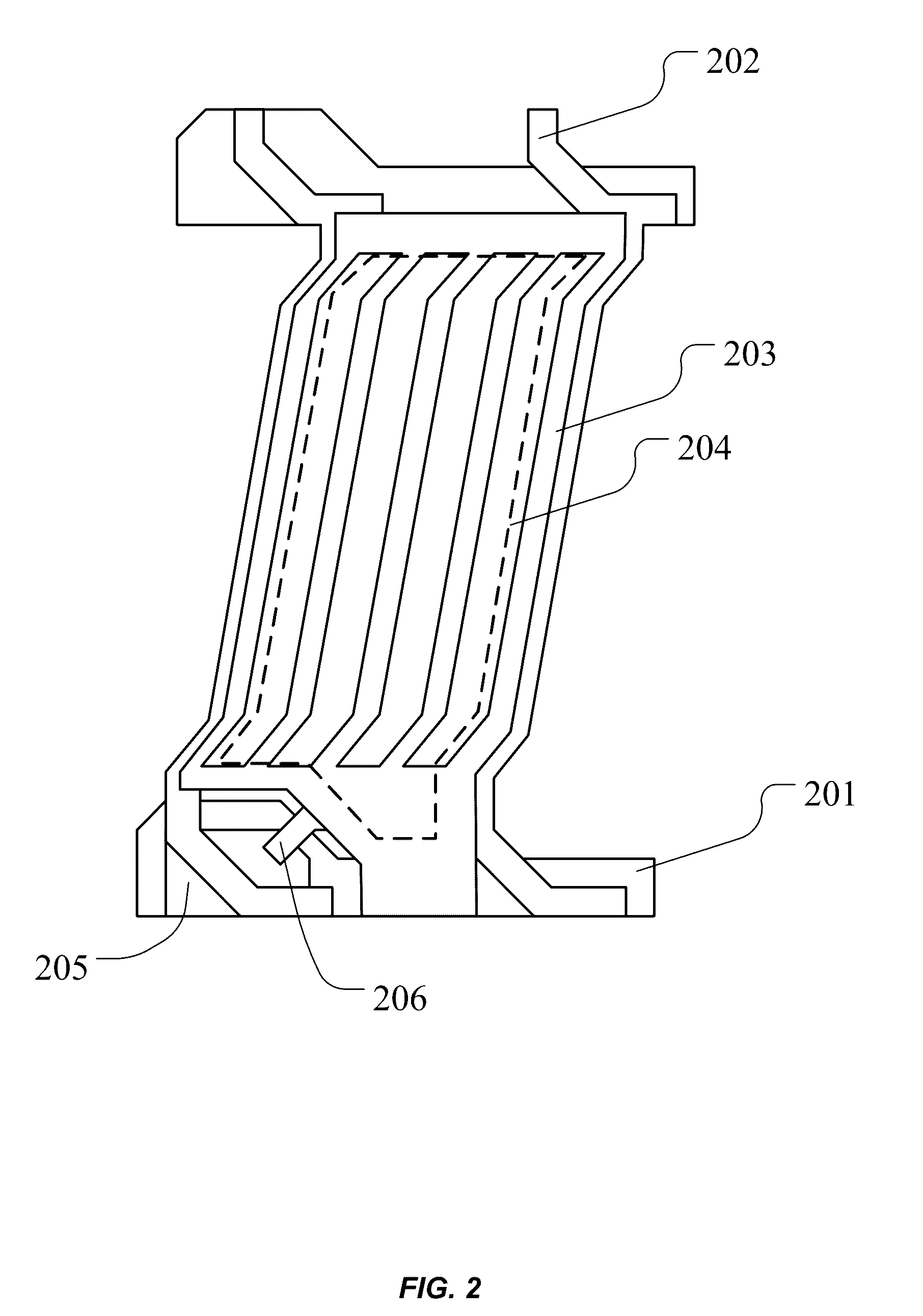
[0031]Referring to FIG. 2, FIG. 3 and FIG. 7, FIG. 7 illustrates a schematic structural diagram in a top view of a liquid crystal display device according to a second embodiment of the present disclosure. The liquid crystal display device according to the second embodiment includes: an array substrate as described above; a color filter substrate as described above; and a liquid crystal layer encapsulated between the array substrate and the color filter substrate.

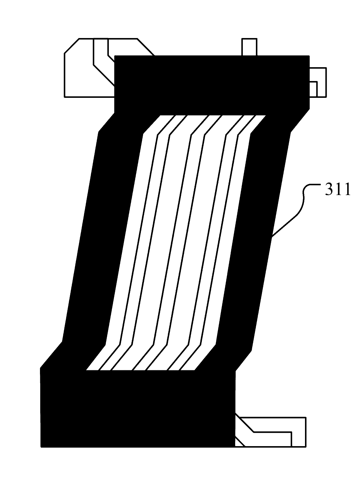
[0032]As illustrated in FIG. 2, the array substrate includes: a substrate; a plurality of scan lines 201 and a plurality of data lines 202 disposed on the substrate intersecting each other and insulated from each other; a plurality of pixel elements defined by the intersection of the scan 201 lines and the data lines 202; a first transparent conductive layer 204 disposed on the substrate; and a second transparent conductive layer 203 disposed on the substrate and in parallel to and insulated from the first transparent conduc...


PUM

PropertyMeasurementUnit
transparent conductiveaaaaaaaaaa
transparentaaaaaaaaaa
sharp angleaaaaaaaaaa

Abstract

The array substrate includes: a substrate; a plurality of scan lines and a plurality of data lines disposed on the substrate intersecting each other to define a plurality of pixel elements and insulated from each other; a first transparent conductive layer disposed on the substrate; and a second transparent conductive layer disposed on the substrate and in parallel to and insulated from the first transparent conductive layer. The data lines, the first transparent conductive layer, and the second transparent conductive layer each comprise a plurality of bended portions, and the bended portions of the second transparent conductive layer are parallel to those of the first transparent conductive layer; additionally or alternatively; the bended portions of the data lines are parallel to those of the first transparent conductive layer or the second transparent conductive layer.

Description

CROSS-REFERENCES TO RELATED APPLICATIONS[0001]This application claims the benefit of priority to Chinese Patent Application No. 201410309487.1, filed with the Chinese Patent Office on Jun. 30, 2014 and entitled “ARRAY SUBSTRATE AND LIQUID CRYSTAL DISPLAY DEVICE”, the content of which is incorporated herein by reference in its entirety.FIELD OF THE DISCLOSURE[0002]The present disclosure relates to liquid crystal display technology, and more particularly to an array substrate and a liquid crystal display device including the array substrate.BACKGROUND OF THE INVENTION[0003]Currently one of predominant displays is a flat panel display. For example, a liquid crystal display device has been widely applied to a computer screen, a mobile phone, a personal digital assistant, a flat panel TV and other electronic products due to its lightweight and thin form factor, low power consumption, no radiation and other advantages.[0004]In order to overcome the drawback of a small angle of view of a l...

Claims


Application Information

Patent Timeline
Patent Type & Authority Patents(United States)
IPC IPC(8): G02F1/136G02F1/1362G02F1/1343H01L27/12
CPCG02F1/136286G02F1/134336G02F1/134363H01L27/124H01L27/1248G02F2001/134372G02F1/134372
Inventor QIN, DANDANCAO, ZHAOKENGWU, YONGJUN
Owner SHANGHAI AVIC OPTOELECTRONICS
Why Eureka
Try Eureka