
Buffer memory for rotating image, image capture device and display device including the same

a technology of rotating images and buffer memory, applied in the field of semiconductor devices, can solve the problems of difficult hardware design of buffer memory, inability to reduce the need to increase the size of buffer memory, so as to achieve the effect of reducing the memory size necessary and facilitating addressing

Active Publication Date: 2013-03-19
SAMSUNG ELECTRONICS CO LTD
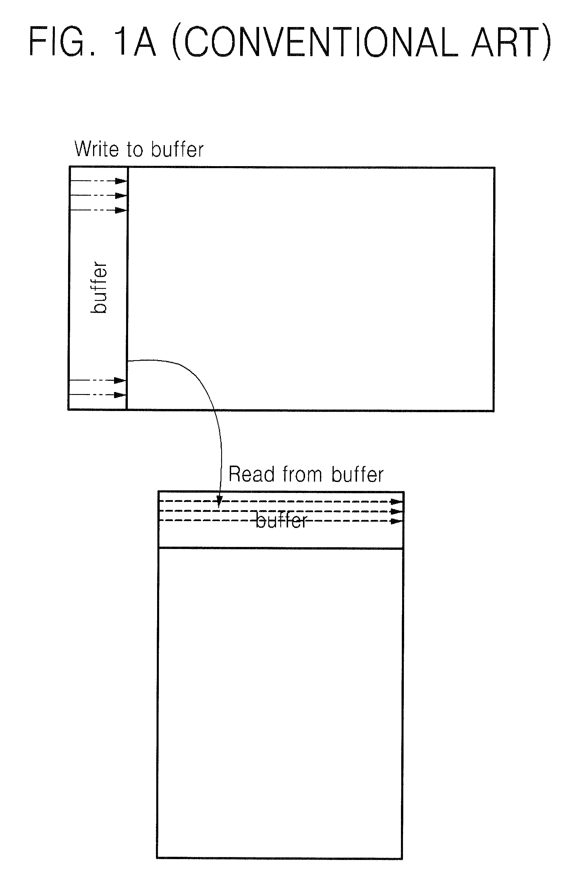
View PDF8 Cites 1 Cited by
  • Summary
  • Abstract
  • Description
  • Claims
  • Application Information

AI Technical Summary

Benefits of technology

The present invention provides a buffer memory that can rotate images while keeping the memory size small and easy to address. It also includes an image capture device and display device with this buffer memory.

Problems solved by technology

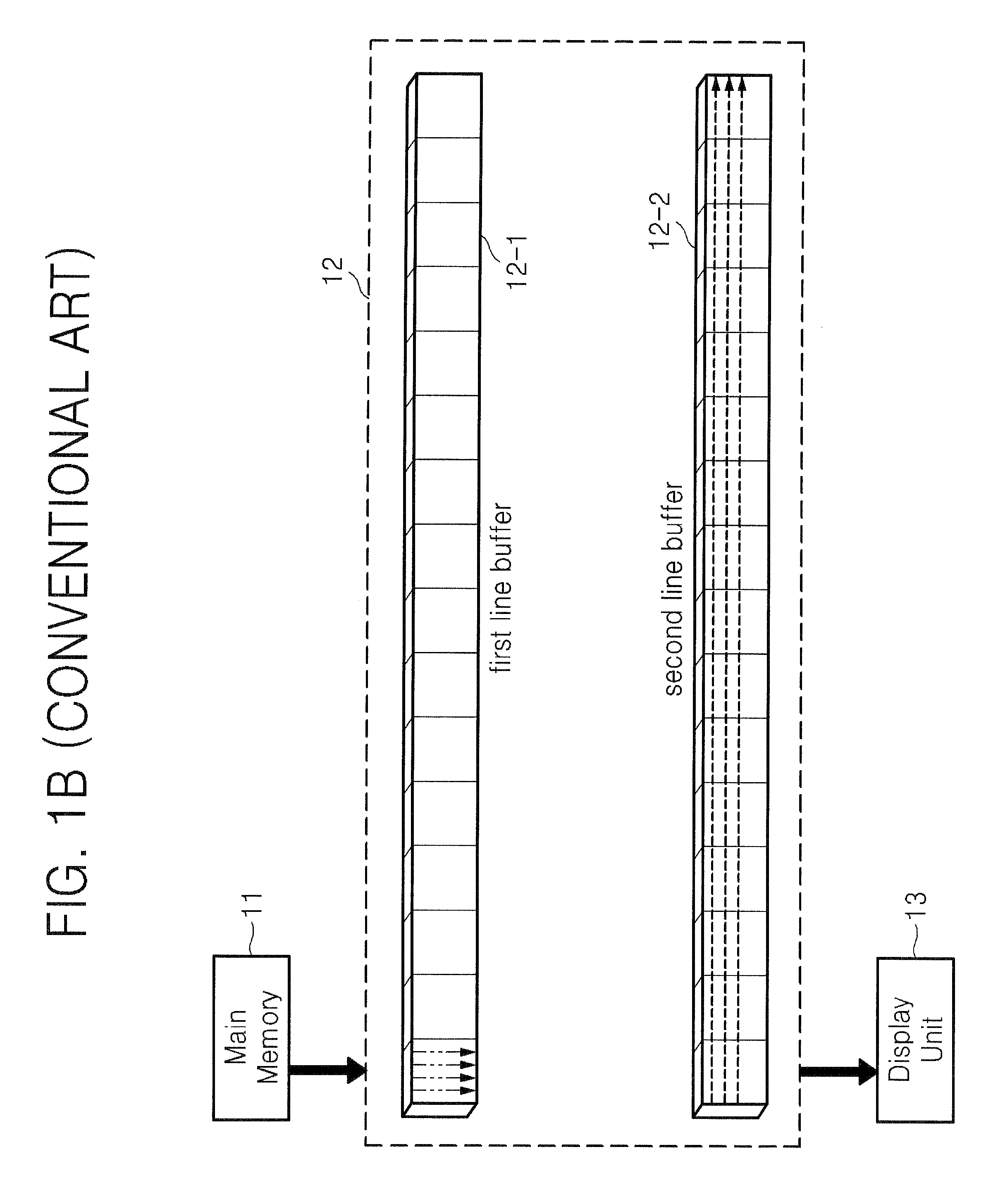
However, to increase the burst size, the size of the buffer memory needs to be increased, which is not desirable for the compactness of the image capture device.
Moreover, conventionally, the size of the buffer memory cannot be decreased and, since a read or write address is not fixed, it is difficult to design the buffer memory in hardware.
This conventional buffering method for image rotation requires a large memory size, and therefore, it does not facilitate the miniaturization of image capture devices or display devices.

Method used


Image

  • Buffer memory for rotating image, image capture device and display device including the same
  • Buffer memory for rotating image, image capture device and display device including the same
  • Buffer memory for rotating image, image capture device and display device including the same

Examples


Embodiment Construction

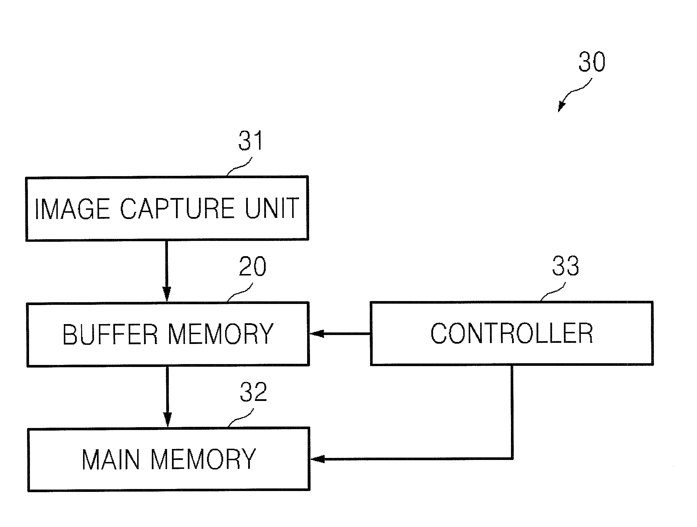
[0028]FIG. 2 is a schematic diagram of a method of forming a buffer memory 20 for rotating an image according to an embodiment of the present invention. For clarity of the description, a 16-line buffer satisfying 32-bit 4-burst transaction and an image having a vertical resolution of 256 are used in the exemplary embodiments of the present invention.

[0029]Unlike the conventional buffer memory for rotating an, image that includes two line buffer memories, the buffer memory 20 according to the current embodiment of the present invention three-dimensionally maps an address using a single line buffer memory and achieves the same effect as that obtained when the two line buffer memories are used. A line buffer memory having a size of 16×256 is divided into 16 macro units having a size of 16×16 and the line buffer memory is subjected to address mapping so that the 16 macro units are stacked. Consequently, the buffer memory 20 having a cube shape can be logically embodied, as illustrated i...


PUM


Abstract

A buffer memory for rotating an image. The buffer memory is address-mapped in three dimensions including a first axis, a second axis, and a third axis, that are orthogonal to one another. Data may be sequentially accessed (read from or written to) the buffer memory in each of the direction of the first axis, the direction of the second axis, and the direction of the third direction. Second data may written to a given plane of the buffer memory at the same time that first data is read from the same plane of the buffer memory.

Description

CROSS-REFERENCE TO RELATED APPLICATIONS[0001]This application claims the priority, under 35 U.S.C. §119, of Korean Patent Application No. 10-2008-0109285, filed on Nov. 5, 2008, the entire contents of which are incorporated by reference herein.BACKGROUND OF THE INVENTION[0002]1. Field of the Invention[0003]The present invention relates to semiconductor devices, and more particularly, to a semiconductor buffer memory having a cube shape that minimizes the memory size needed for image rotation and to allow addressing to be performed with a simple logic, and an image capture device and display device including the same.[0004]2. Description of the Related Art[0005]When an image capture device (e.g., a digital camera) rotates a captured image to store it in a main memory or rotates an image stored in the main memory to display it, conventionally a two-line memory buffer may be used. For instance, to rotate a 1024×768 image by 90 degrees with a 32-bit bus and 4-burst transaction, a 2×16×7...

Claims


Application Information

Patent Timeline
Patent Type & Authority Patents(United States)
IPC IPC(8): H04N5/76
CPCG09G5/393G09G5/395H04N5/772G09G2340/0492H04N5/907H04N21/433
Inventor LIM, EUI CHEOL
Owner SAMSUNG ELECTRONICS CO LTD
Learn More