
Method of storing data on a flash memory device

a flash memory and data technology, applied in the field of flash memory devices, can solve the problem that the data values in the memory cells cannot be selectively changed, and achieve the effect of improving the storage efficiency and reducing the cost of storag

Active Publication Date: 2011-05-24
MICRON TECH INC
View PDF12 Cites 16 Cited by
  • Summary
  • Abstract
  • Description
  • Claims
  • Application Information

AI Technical Summary

Benefits of technology

The patent text describes a type of memory device called NAND flash memory, which is commonly used in solid state disks (SSDs) and other applications. The invention relates to improving the performance of NAND flash memory devices by allowing for selective erasure and programming of memory cells within a memory block. This reduces the time and resources required for erasure and programming, and improves the speed and efficiency of NAND flash memory devices.

Problems solved by technology

Likewise, when changing data values in some of memory cells in a memory block, the data values in the memory cells cannot be selectively changed.

Method used


Image

  • Method of storing data on a flash memory device
  • Method of storing data on a flash memory device
  • Method of storing data on a flash memory device

Examples


Embodiment Construction

[0023]In certain applications (for example, when a NAND flash memory serves as a solid state disk), data is frequently written or modified on a NAND flash memory. Thus, at least some memory blocks in the NAND flash memory are subjected to a great number of programming cycles.

[0024]In a conventional write method, data is written on a memory block in a bottom-up fashion, starting from memory cells on or near the lowermost (or bottom) word line. Then, data is sequentially written page-by-page on memory cells on word lines above the lowermost word line until memory cells on the uppermost (or top) word line are filled up. For example, data is written first on memory cells 110 on the lowermost word line WL0, and last on memory cells 110 on the uppermost word line WLn in FIG. 2C. In other instances, data may be written first on memory cells 110 on the second lowermost word line WL1, then memory cells 110 on the lowermost word line WL0, and may be written on memory cells 110 on word lines a...


PUM


Abstract

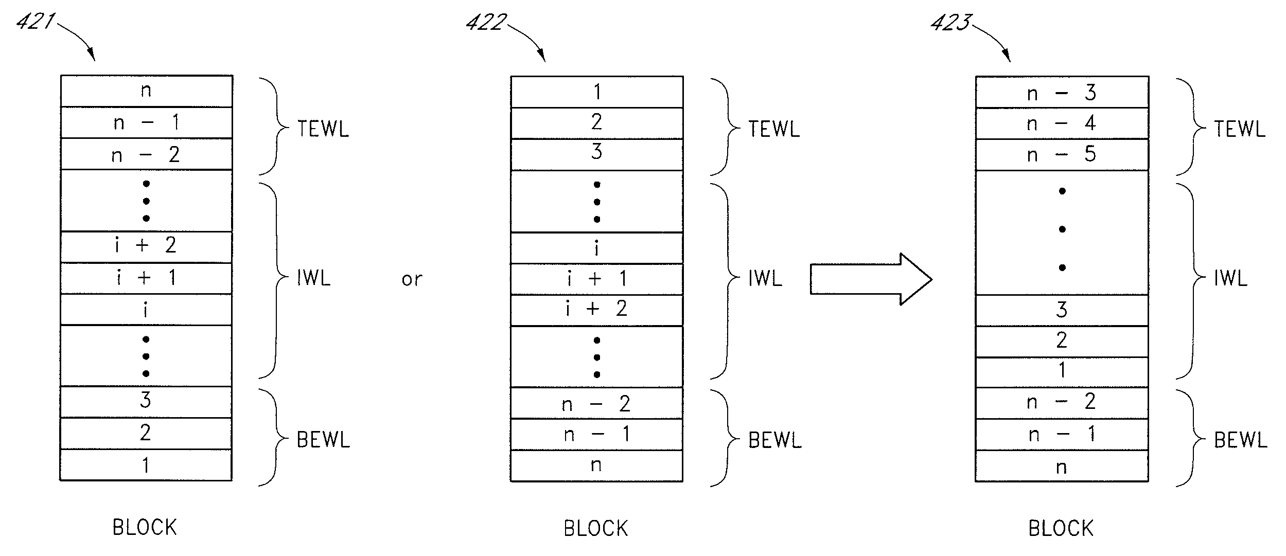
Methods and apparatus are disclosed, such as those involving a flash memory device. One such method includes storing data on memory cells on a memory block including a plurality of word lines and a plurality of memory cells on the word lines. The word lines comprising one or more bottom edge word lines, one or more top edge word lines, and intermediate word lines between the bottom and top edge word lines. The data is stored first on memory cells on the intermediate word lines. Then, a remaining portion, if any, of the data is stored on memory cells on the bottom edge word lines and / or the top edge word lines. This method enhances the life of the flash memory by preventing a premature failure of memory cells on the bottom or top edge word lines, which can be more prone to failure.

Description

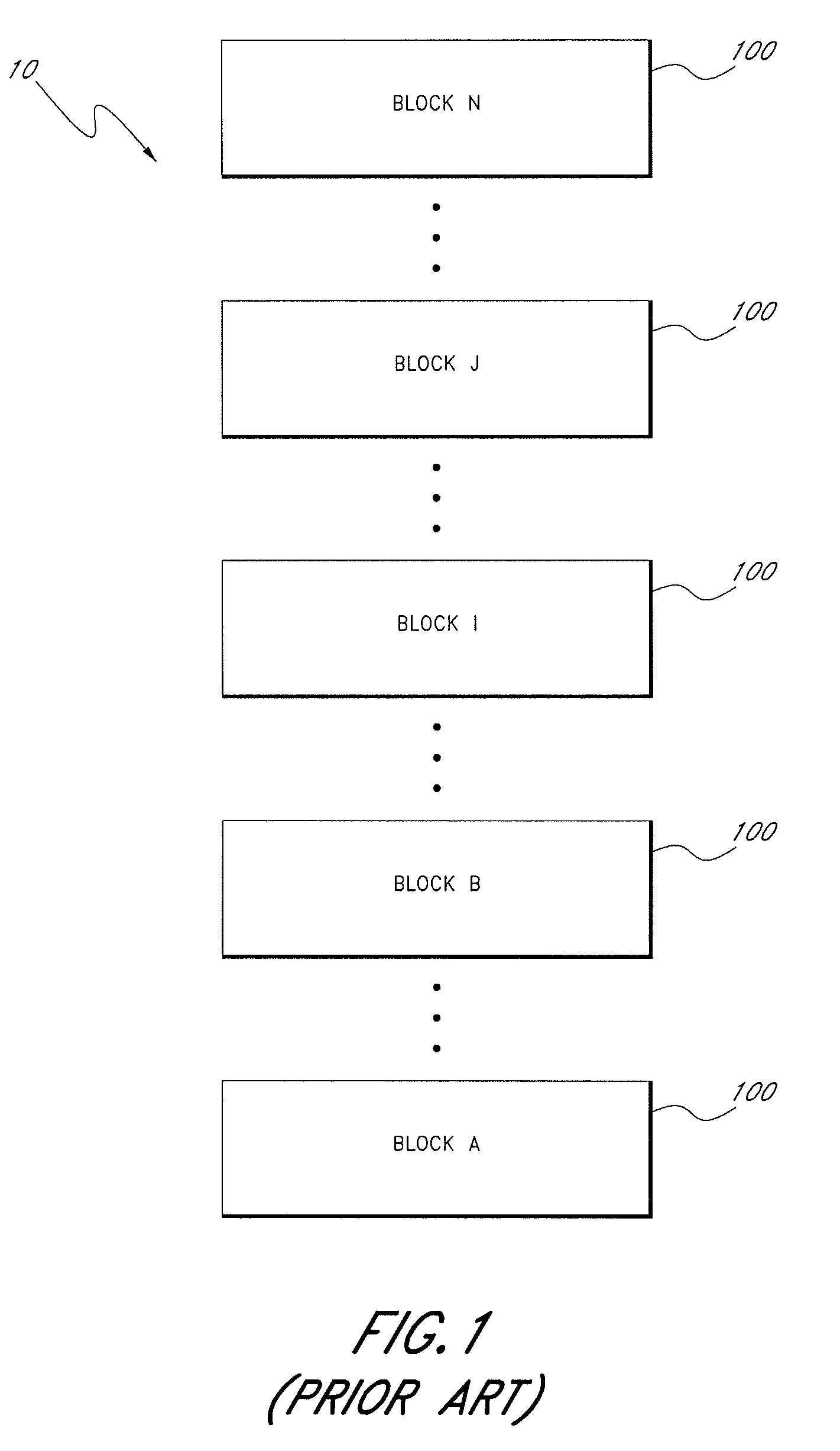
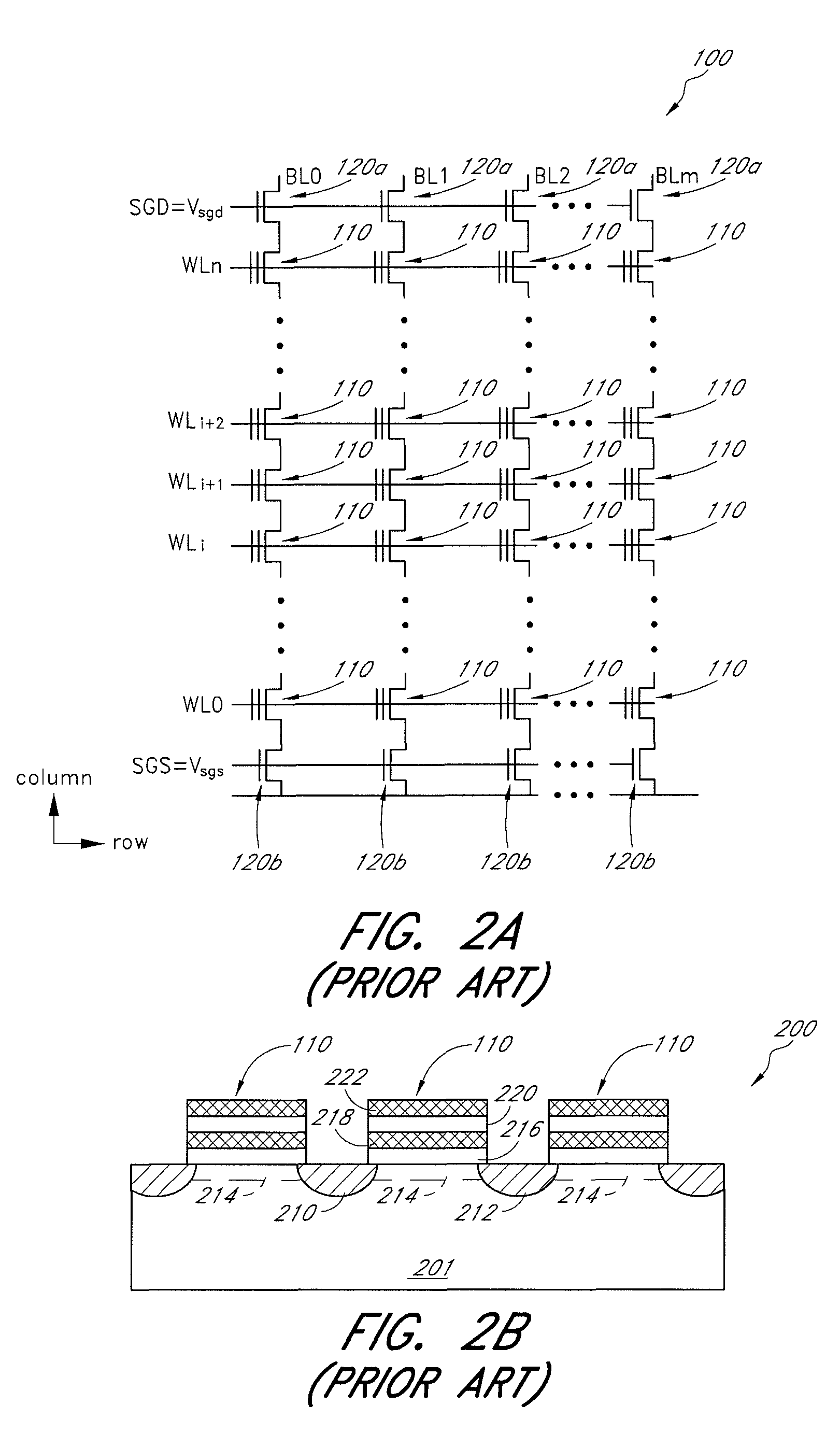
BACKGROUND[0001]1. Field of the Invention[0002]Embodiments of the invention relate to memory devices, and more particularly, in one or more embodiments, to flash memory devices.[0003]2. Description of the Related Art[0004]Flash memory devices are non-volatile memory devices which store information on a semiconductor in a way that needs no power to maintain the information stored therein. Among flash memory devices, NAND flash memory devices have been widely used as mass-storage devices because of their high storage densities and low costs. In some applications, a NAND flash memory device serves as a solid state disk (SSD), replacing or supplementing a hard disk.[0005]Referring to FIG. 1, a conventional NAND flash memory device includes a plurality of memory blocks. The illustrated flash memory device 10 includes first to N-th memory blocks 100. Each of the memory blocks 100 includes a plurality of memory cells arranged in a matrix form.[0006]FIG. 2A illustrates one of the memory blo...

Claims


Application Information

Patent Timeline
Patent Type & Authority Patents(United States)
IPC IPC(8): G06F13/00G11C16/04G11C11/34G06F13/28
CPCG11C8/08G11C16/3495G11C16/10G11C2216/14G11C16/06G11C16/08
Inventor HAN, JIN-MAN
Owner MICRON TECH INC
Learn More