
OLED electron-injecting layer

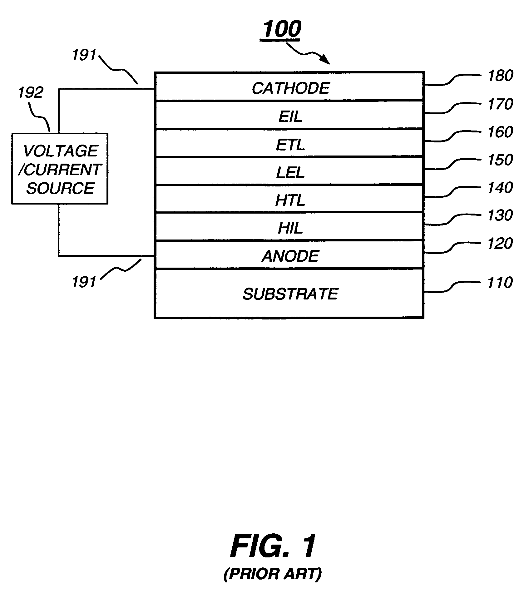
a technology of electron injection and oled, which is applied in the direction of discharge tube luminescnet screen, other domestic articles, natural mineral layered products, etc., can solve the problems of insufficient electron recombination in lel, unbalanced electron-hole recombination, and difficult or impossible electron injection from the etl into the lel

Active Publication Date: 2009-12-08
GLOBAL OLED TECH
View PDF12 Cites 43 Cited by
  • Summary
  • Abstract
  • Description
  • Claims
  • Application Information

AI Technical Summary

Benefits of technology

[0016]The present invention makes use of a second electron-injecting layer including an organic material having a reduction potential greater than −1.0 eV in direct contact with the cathode and forming a stable interface between the cathode and this layer with no electron injection barrier from the cathode into the electron-injecting layer. It is an advantage of the present invention that the OLED with the second electron-injecting layer can not only increase the lifetime but also reduce the voltage rise during operation, which is useful for making high quality active matrix OLED display and other electronic devices. It is another advantage of the present invention that a stable metal, such as Ag, Au, Al, and Cu, can be used to form the cathode. These stable metals do not readily react with water or oxygen to form dark spots in the OLEDs.
that the OLED with the second electron-injecting layer can not only increase the lifetime but also reduce the voltage rise during operation, which is useful for making high quality active matrix OLED display and other electronic devices. It is another advantage of the present invention that a stable metal, such as Ag, Au, Al, and Cu, can be used to form the cathode. These stable metals do not readily react with water or oxygen to form dark spots in the OLEDs.

Problems solved by technology

As is known, electron transport in OLED is generally less efficient than hole transport.
As a result, the electron-hole recombination in LEL is sometimes unbalanced with insufficient electrons.
Electron injection from the ETL into the LEL would be very difficult or impossible, resulting in little or no EL emission from the OLED.

Method used


Image

  • OLED electron-injecting layer
  • OLED electron-injecting layer
  • OLED electron-injecting layer

Examples


example 6 (

Inventive)

[0162]An OLED in accordance with the present invention was constructed as the same as that in Example 4, except that the layer c in Example 4 was replaced by:[0163]c) the 1st EIL, 29 nm thick, composed of Alq doped with about 1.2 vol % lithium; and[0164]d) the 2nd EIL, 1 nm thick, composed of HAT-CN.

[0165]This OLED, having the 2nd EIL in direct contact with the 1st EIL, requires a drive voltage of about 5.0 V to pass 20 mA / cm2. Under this test condition, the device has a luminance of 1891 cd / m2, and a luminous efficiency of about 9.5 cd / A. Its emission peak is at 521 nm. The operational lifetime, measured as T50(RT@80 mA / cm2), is about 312 hours. The average rate of the voltage rise during the lifetime testing is about 3.5 mV / hr. Its normalized luminance vs. operational time and its drive voltage vs. operational time, tested at room temperature and at 80 mA / cm2, are shown in FIGS. 6 and 7, respectively.

[0166]FIGS. 6 and 7 demonstrate that the OLED constructed in accordance...

example 7 (

Inventive)

[0167]Another OLED in accordance with the present invention was constructed in the same general manner as that in Example 1. But, the layer structure of the EL unit is as follows:[0168]a) an HIL, 10 nm thick, composed of HAT-CN;[0169]b) an HTL, 65 nm thick, composed of NPB;[0170]c) a LEL, 30 nm thick, composed of Alq doped with 1.0 vol % C545T;[0171]d) the 1st EIL, 20 nm thick, composed of Alq doped with about 1.2 vol % lithium; and[0172]e) the 2nd EIL, 10 nm thick, composed of HAT-CN.

[0173]This OLED requires a drive voltage of about 5.1 V to pass 20 mA / cm2. Under this test condition, the device has a luminance of 1823 cd / m2, and a luminous efficiency of about 9.1 cd / A. Its emission peak is at 521 nm. The operational lifetime, measured as T50(RT@80 mA / cm2), is about 350 hours. The average rate of the voltage rise during the lifetime testing is about 2.9 mV / hr. Its normalized luminance vs. operational time and its drive voltage vs. operational time, tested at room temperatu...

example 8 (

Inventive)

[0174]Another OLED was constructed in accordance with the present invention. This OLED is the same as that in Example 7, except that layers d and e were changed as follows:[0175]d) the 1st EIL, 5 nm thick, composed of Alq doped with about 1.2 vol % lithium; and[0176]e) the 2nd EIL, 25 nm thick, composed of HAT-CN doped with about 1.2 vol % lithium.

[0177]This OLED requires a drive voltage of about 4.6 V to pass 20 mA / cm2. Under this test condition, the device has a luminance of 1898 cd / m2, and a luminous efficiency of about 9.5 cd / A. Its emission peak is at 521 nm. The operational lifetime, measured as T50(RT@80 mA / cm2), is about 330 hours. The average rate of the voltage rise during the lifetime testing is about 2.1 mV / hr. Its normalized luminance vs. operational time and its drive voltage vs. operational time, tested at room temperature and at 80 mA / cm2, are shown in FIGS. 8 and 9, respectively.

[0178]It is evident from FIGS. 8 and 9 that the OLEDs having a Li-doped HAT-CN...


PUM

PropertyMeasurementUnit
reduction potentialaaaaaaaaaa
optical band gapaaaaaaaaaa

Abstract

An OLED includes an anode, a light-emitting layer disposed over the anode, and a first electron-injecting layer disposed over the light-emitting layer, wherein the first electron-injecting layer includes at least one organic host material having a reduction potential less than −1.0 V vs. a Saturated Calomel Electrode and at least one dopant material capable of reducing the organic host material. The OLED also includes a second electron-injecting layer disposed in contact with the first electron-injecting layer, wherein the second electron-injecting layer includes at least one organic material having a reduction potential greater than −1.0 V vs. a Saturated Calomel Electrode, and a cathode disposed over the second electron-injecting layer.

Description

CROSS REFERENCE TO RELATED APPLICATIONS[0001]Reference is made to commonly assigned U.S. patent application Ser. No. 10 / 824,086 filed Apr. 14, 2005 (now U.S. Pat. No. 7,192,659) by Michele L. Ricks et al., entitled “OLED Device Using Reduced Drive Voltage”; commonly assigned U.S. patent application Ser. No. 11 / 111,386 filed Apr. 21, 2005 (U.S. Patent Application Publication No. 2006 / 0240281) by Liang-Sheng Liao et al., entitled “Contaminant-Scavenging Layer on OLED Anodes”; and U.S. patent application Ser. No. 11 / 111,367 filed Apr. 21, 2005 (U.S. Patent Application Publication No. 2006 / 0240280) by Liang-Sheng Liao et al., entitled “OLED Anode Modification Layer”, the disclosures of which are herein incorporated by reference.FIELD OF INVENTION[0002]The present invention relates to an organic light-emitting device (OLED) in which an organic material having a strong oxidizing property is used in an electron-injecting layer of the device.BACKGROUND OF THE INVENTION[0003]OLEDs, as descri...

Claims


Application Information

Patent Timeline
Patent Type & Authority Patents(United States)
IPC IPC(8): H01L51/54
CPCH01L51/0051H01L51/0067H01L51/5052H01L51/5092H01L51/0071H01L51/0053Y10S428/917Y10T428/24942H10K85/611H10K85/621H10K85/654H10K85/657H10K50/165H10K50/171
Inventor LIAO, LIANG-SHENGSLUSAREK, WOJCIECH K.RICKS, MICHELE L.YOUNG, RALPH H.COMFORT, DUSTIN L.
Owner GLOBAL OLED TECH
Learn More