Liquid crystal display and display

a liquid crystal display and display panel technology, applied in non-linear optics, instruments, optics, etc., can solve the problems of deterioration of glass substrate strength, difficulty in achieving both thickness reduction and ensuring a sufficient strength, and achieve sufficient strength and sufficient strength. , the effect of reducing the thickness of each glass substra

Active Publication Date: 2009-05-12
JAPAN DISPLAY INC +1
View PDF8 Cites 11 Cited by
  • Summary
  • Abstract
  • Description
  • Claims
  • Application Information

AI Technical Summary

Benefits of technology

[0011]Moreover, the method of using a plastic substrate instead of the glass substrate poses the problem that the heat resistance and solvent resistance (chemicals resistance) of the plastic substrate are low in comparison with the glass substrate and that therefore the handling of the plastic substrate is difficult for example in the step of forming TFT onto the glass substrate. Further, in the case of a liquid crystal display panel using a glass substrate as the TFT substrate and a plastic substrate as the counter substrate, unevenness in display easily occurs because the substrates differ in the amount of deformation caused by changes of environmental conditions such as temperature and humidity.
[0076]In the case of installing the liquid crystal display of the third or the fourth invention into a mobile telephone terminal, it is preferable that a protective cover for protecting the liquid crystal display panel be affixed to a sheath of the mobile telephone terminal as in the conventional liquid crystal display. However, in the liquid crystal displays of third and fourth inventions, the total thickness of the first and second substrates is not larger than 0.5 mm and the thickness of the resin film is 0.1 mm or more and 0.3 mm or less. That is, in each of the liquid crystal displays of the third and fourth inventions, since the liquid crystal display panel is thinner than the conventional liquid crystal display panel, the thickness of the liquid crystal display can be so much reduced. Consequently, even if the protective cover for protecting the liquid crystal display panel is affixed to the sheath of the mobile telephone terminal, it is possible to reduce the thickness of the display unit of the mobile telephone terminal in comparison with the conventional counterpart.

Problems solved by technology

In the liquid crystal display, when the thickness of the glass substrate used in the TFT substrate or the counter substrate is reduced by polishing in order to reduce the thickness of the liquid crystal display panel, the strength of the glass substrate is deteriorated and the strength of the liquid crystal display panel is also deteriorated.
Thus, the method of polishing the glass substrate to reduce the substrate thickness poses the problem that it is difficult to attain both thickness reduction and ensuring of a sufficient strength.
Moreover, the method of using a plastic substrate instead of the glass substrate poses the problem that the heat resistance and solvent resistance (chemicals resistance) of the plastic substrate are low in comparison with the glass substrate and that therefore the handling of the plastic substrate is difficult for example in the step of forming TFT onto the glass substrate.
Further, in the case of a liquid crystal display panel using a glass substrate as the TFT substrate and a plastic substrate as the counter substrate, unevenness in display easily occurs because the substrates differ in the amount of deformation caused by changes of environmental conditions such as temperature and humidity.

Method used


Image

  • Liquid crystal display and display
  • Liquid crystal display and display
  • Liquid crystal display and display

Examples


first embodiment

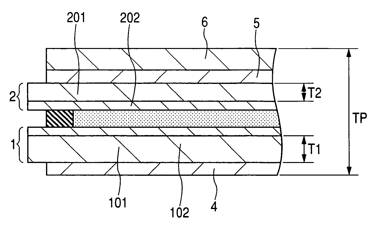
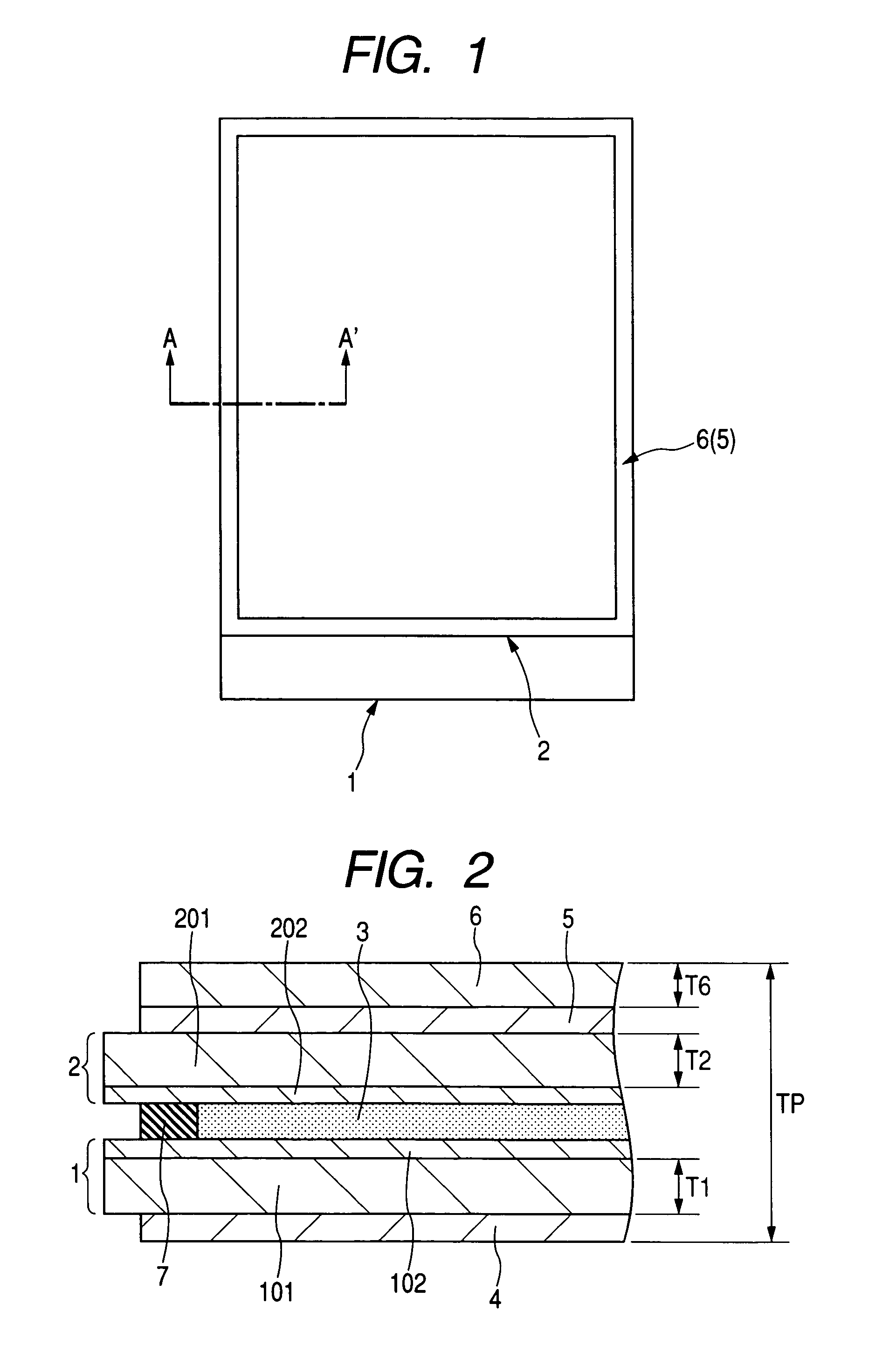
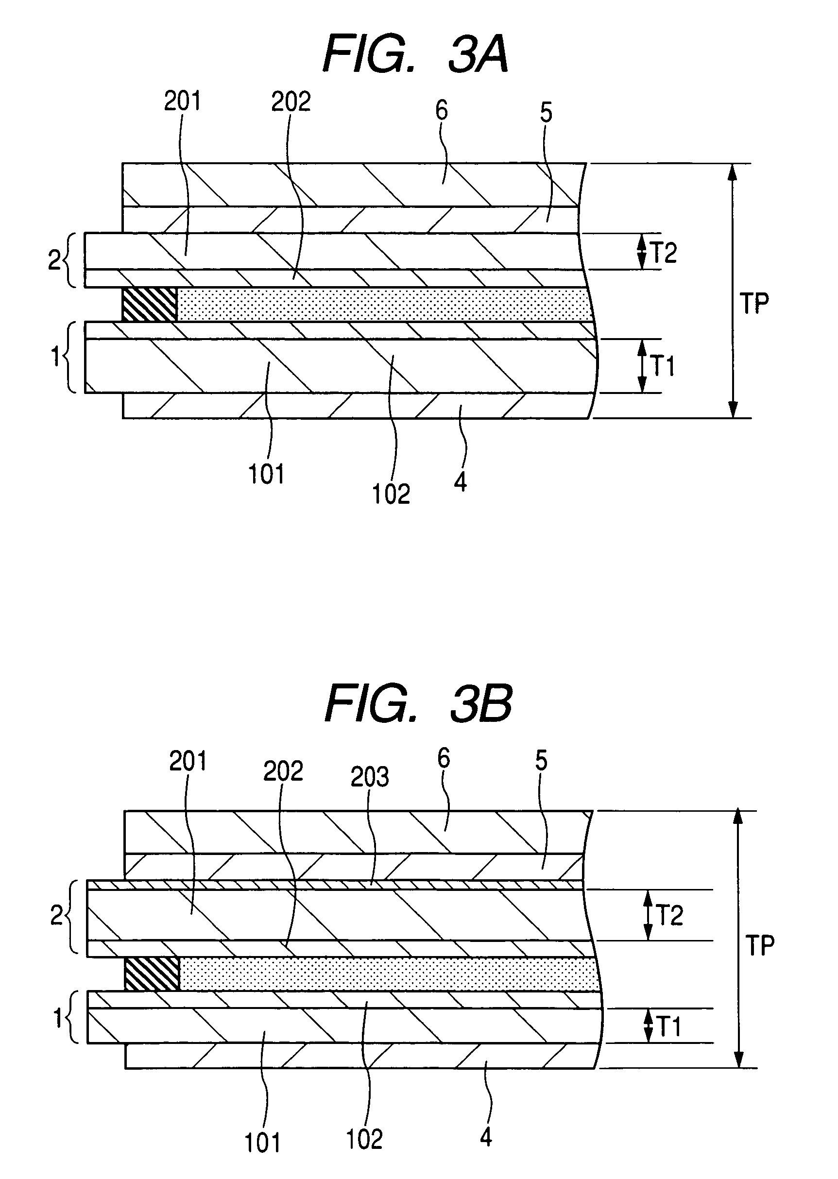
[0099]FIG. 1 is a schematic plan view showing a schematic configuration of a liquid crystal display panel according to a first embodiment of the present invention, FIG. 2 is a sectional view taken along the line A-A′ of FIG. 1, and FIG. 3 is a schematic sectional view for explaining a function and effect of the liquid crystal display panel of the first embodiment. In FIG. 3 there are shown two sectional views as FIG. 3A and FIG. 3B, both of which correspond to the sectional configuration taken along the line A-A′ in FIG. 1.

[0100]In the first embodiment, a reference will be made to a transmission type liquid crystal display as an example of a display to which the present invention is applied, and a description will be given below about the configuration, as well as function and effect, of a liquid crystal display panel used in the transmission type liquid crystal display.

[0101]As shown in FIG. 1, the liquid crystal display panel of the first embodiment includes a TFT substrate 1, a c...

second embodiment

[0143]FIG. 12 is a schematic sectional view showing a schematic configuration of a liquid crystal display panel according to a second embodiment of the present invention. The sectional view of FIG. 12 corresponds to the sectional configuration taken along the line A-A′ of FIG. 1.

[0144]The liquid crystal display panel of the second embodiment is basically of the same configuration as the liquid crystal display panel of the first embodiment. In the second embodiment, therefore, a description will be given below about only the difference from the first embodiment.

[0145]For example as shown in FIG. 12, the liquid crystal display panel of the second embodiment includes a TFT substrate 1, a counter substrate 2, a liquid crystal material 3 held between the TFT substrate 1 and the counter substrate 2, a pair of polarizing plates (a lower polarizing plate 4 and an upper polarizing plate 5) disposed between the TFT substrate 1 and the counter substrate 2 both holding the liquid crystal materi...

third embodiment

[0169]FIG. 16 is a schematic sectional view showing a schematic configuration of a liquid crystal display panel according to a third embodiment of the present invention.

[0170]The liquid crystal display panel of the third embodiment is basically of the same configuration as the liquid crystal display panel of the first embodiment. In the third embodiment, therefore, a description will be given only about points different from the first embodiment.

[0171]For example as shown in FIG. 16, the liquid crystal display panel of the third embodiment includes a TFT substrate 1, a counter substrate 2, a liquid crystal material 3 held between the TFT substrate and the counter substrate 2, a pair of polarizing plates (a lower polarizing plate 4 and an upper polarizing plate 5) disposed between the TFT substrate 1 and the counter substrate 2 both holding the liquid crystal material 3, and a resin film 6 affixed in contact with the lower polarizing plate 4 located on the TFT substrate 1 side.

[0172]...


PUM

PropertyMeasurementUnit
thicknessaaaaaaaaaa
thicknessaaaaaaaaaa
thicknessaaaaaaaaaa

Abstract

A liquid crystal display comprises a liquid crystal display panel, the liquid crystal display panel comprising a first substrate; a second substrate disposed on an observer side with respect to the first substrate and opposed to the first substrate; a liquid crystal held between the first substrate and the second substrate; an upper polarizing plate disposed on the observer side with respect to the second substrate; and a resin film disposed on the observer side with respect to the upper polarizing plate and affixed in contact with the upper polarizing plate, the resin film being higher in surface hardness than the upper polarizing plate. Both reduction in thickness of the liquid crystal display panel and ensuring of a sufficient strength are attained.

Description

CLAIM OF PRIORITY[0001]The present application claims priority from Japanese Application JP 2005-372185 filed on Dec. 26, 2005, the content of which is hereby incorporated by reference into this application.BACKGROUND OF THE INVENTION[0002]1. Field of the Invention[0003]The present invention relates to a liquid crystal display and a display. In particular, the present invention is concerned with a technique applicable effectively to a liquid crystal display (module) used in a hand-held electronic device such as a mobile telephone terminal.[0004]2. Description of the Related Art[0005]A thin display such as a liquid crystal display has been conventionally used for a display used in a hand-held electronic device such as a mobile telephone terminal or a PDA (Personal Digital Assistant).[0006]The liquid crystal display is a display having a liquid crystal display panel comprising a pair of substrates and a liquid crystal material held therebetween. One of the paired substrates is general...

Claims


Application Information

Patent Timeline
Patent Type & Authority Patents(United States)
IPC IPC(8): G02F1/1335
CPCG02F1/1333G02F1/133536G02F1/133528G02F1/133308G02F1/133608G02F2201/50G02F1/1339
Inventor FUKUDA, KOICHI
Owner JAPAN DISPLAY INC
Why Eureka
Try Eureka