
Imaging apparatus and control circuit of imaging device

a control circuit and imaging device technology, applied in the field of imaging devices, can solve the problems of disadvantageous increase of the agc circuit and the dgc circuit in maintaining the s/n ratio, and small influence of time on the increase of noise, so as to prevent the deterioration of the signal-to-noise ratio

Active Publication Date: 2008-11-25
SEMICON COMPONENTS IND LLC
View PDF10 Cites 10 Cited by
  • Summary
  • Abstract
  • Description
  • Claims
  • Application Information

AI Technical Summary

Benefits of technology

[0010]Accordingly, the invention has been made up to solve the above-mentioned problems, and it is an object of the present invention to provide exposure control which can ensure a frame rate and adequately prevent an S / N ratio from deteriorating in an imaging apparatus.

Problems solved by technology

Accordingly, an influence of a noise component due to a dark current or random noise included in the image signal increases and thus an S / N ratio (signal to noise ratio) is deteriorated.
On the contrary, the expansion of the exposure time has a small influence on the increase of the noise.
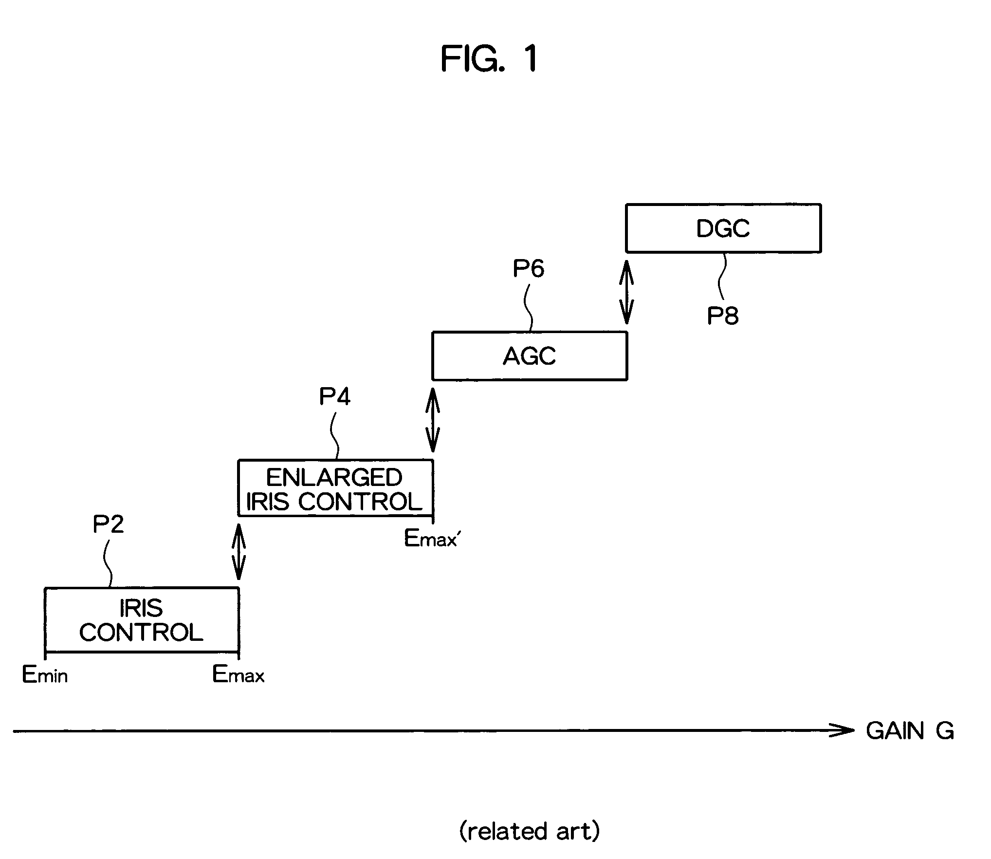
As described above, when the level of the image signal is increased, the increase of the gains of the AGC circuit and the DGC circuit is disadvantageous in maintaining the S / N ratio.
But, in photographing a moving image or preview, the above-mentioned technology may be disadvantageous, because it is important that the image is smoothly in accordance with the motion of the subject.

Method used


Image

  • Imaging apparatus and control circuit of imaging device
  • Imaging apparatus and control circuit of imaging device
  • Imaging apparatus and control circuit of imaging device

Examples


Embodiment Construction

[0020]Hereinafter, preferred embodiments of the present invention will now be described with reference to the accompanying drawings.

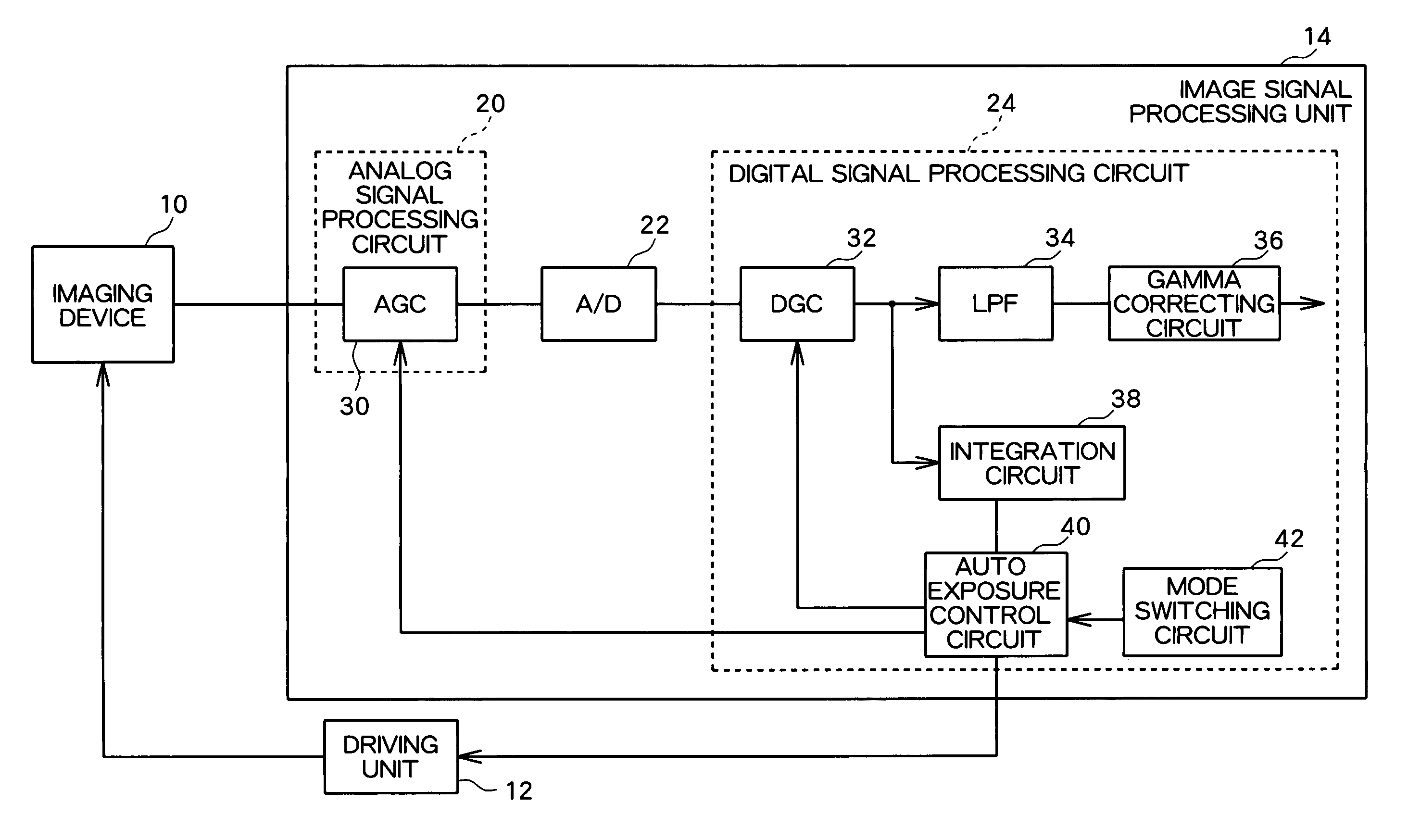
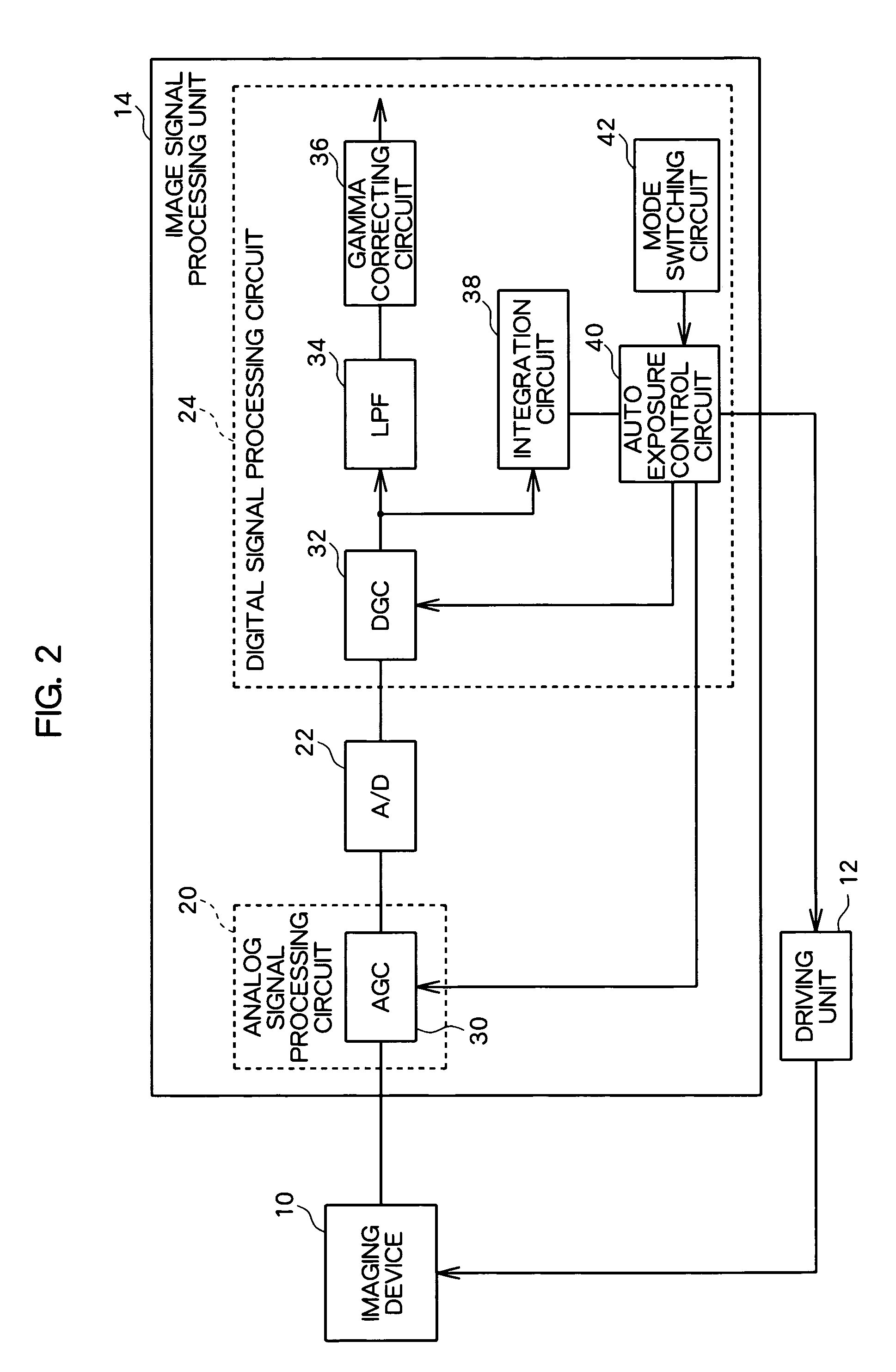
[0021]FIG. 2 is a block diagram schematically illustrating the structure of an imaging apparatus according to an embodiment of the present invention. This imaging apparatus includes an imaging device 10, such as a CCD image sensor, a driving unit 12 for driving the imaging device 10, and an image signal processing unit 14. As described below, the driving unit 12 and the image signal processing unit 14 have a control circuit function for controlling a level of an image signal obtained from the imaging device 10.

[0022]The image signal processing unit 14 generates a luminance signal based on the image signal output from the imaging device 10 to output it to a display device (not shown) and determines the exposure state to control the driving unit 12 for driving the imaging device 10. The image signal input from the imaging device 10 to the image signal pro...


PUM


Abstract

In exposure control of an imaging apparatus, if a vertical scanning period is enlarged to increase an exposure time when the exposure time reaches an upper limit value, there occurs a problem in that a frame rate is reduced. Accordingly, when a subject is dark, an auto exposure control circuit sets the vertical scanning period V to a standard value Vst, increases the exposure time E to the upper limit value Emax (P60) and then increases a gain α of an AGC circuit (P62). If the image is still dark even when the gain α reaches the upper limit value α max, the auto exposure control circuit switches the vertical scanning period V to an enlarged value Vex and thus more increases the exposure time E (P64).

Description

FIELD OF THE INVENTION[0001]The present invention relates to an imaging apparatus for photographing a subject, and more particularly, to an exposure control for controlling a level of an image signal in accordance with brightness of a subject.BACKGROUND OF THE INVENTION[0002]In an imaging apparatus, such as a digital camera, an image signal output from an image device, such as a CCD (charge coupled device) image sensor, has a low signal level when a subject is dark. Accordingly, an influence of a noise component due to a dark current or random noise included in the image signal increases and thus an S / N ratio (signal to noise ratio) is deteriorated. On the other hand, if the subject is bright and the signal level is high, a dynamic range of the image signal is suppressed by saturation of a light receiving pixel, a CCD shift register or the like.[0003]For this reason, in order to maintain the signal level of the obtained image signal in a preferable range even in a case in which the ...

Claims


Application Information

Patent Timeline
Patent Type & Authority Patents(United States)
IPC IPC(8): G03B7/00H04N5/235H04N5/238H04N5/243H04N5/335H04N5/353H04N5/376H04N101/00
CPCH04N5/2352H04N5/2353H04N5/243H04N23/72H04N23/73H04N23/76H04N23/70
Inventor TANIMOTO, TAKASHINAKAI, TOMOMICHI
Owner SEMICON COMPONENTS IND LLC
Learn More