Embedded leadframe semiconductor package

a semiconductor package and leadframe technology, applied in semiconductor devices, semiconductor/solid-state device details, electrical devices, etc., can solve the problems of absence of elements, and achieve the effect of effective electrical isolation of leads

Active Publication Date: 2007-03-13
AMKOR TECH SINGAPORE HLDG PTE LTD
View PDF378 Cites 73 Cited by
  • Summary
  • Abstract
  • Description
  • Claims
  • Application Information

AI Technical Summary

Benefits of technology

[0007]After both the leadframe and the semiconductor die have been mounted to the substrate and electrically connected to the conductive pattern thereof, a molding operation is completed wherein a mold cap or package body is formed to fully cover or encapsulate the semiconductor die and conductive wires (if any), and partially cover or encapsulate the leadframe. Subsequent to the completion of the overmold, a deflashing process is completed to fully expose portions of the leads of the leadframe upon the top surface of the package body. Thereafter, the exposed portions of the leads may optionally be plated with a layer of a suitable conductive material. An etching or sawing process is then completed to effectively electrically isolate the leads of the leadframe from each other. The exposed portions of the leads of the leadframe (which define pads or terminals) provide a footprint to which a second semiconductor package may be electrically connected, and thus stacked upon the package.

Problems solved by technology

One of the notable drawbacks of currently known BGA packages is the absence therein of any elements which allow for the stacking of a second semiconductor package thereon.

Method used


Image

  • Embedded leadframe semiconductor package
  • Embedded leadframe semiconductor package
  • Embedded leadframe semiconductor package

Examples


Embodiment Construction

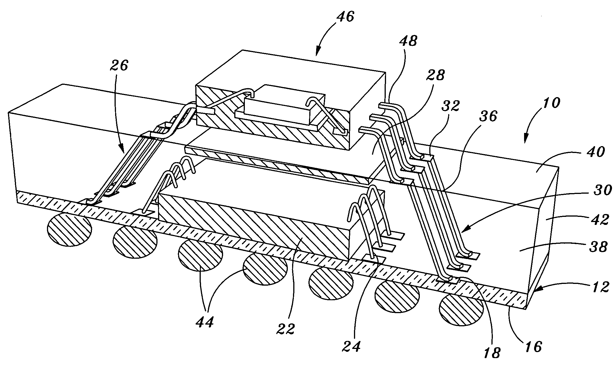
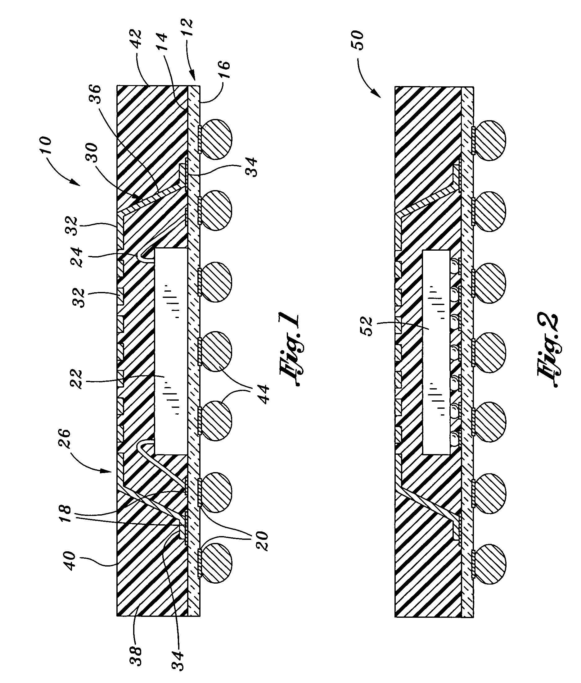
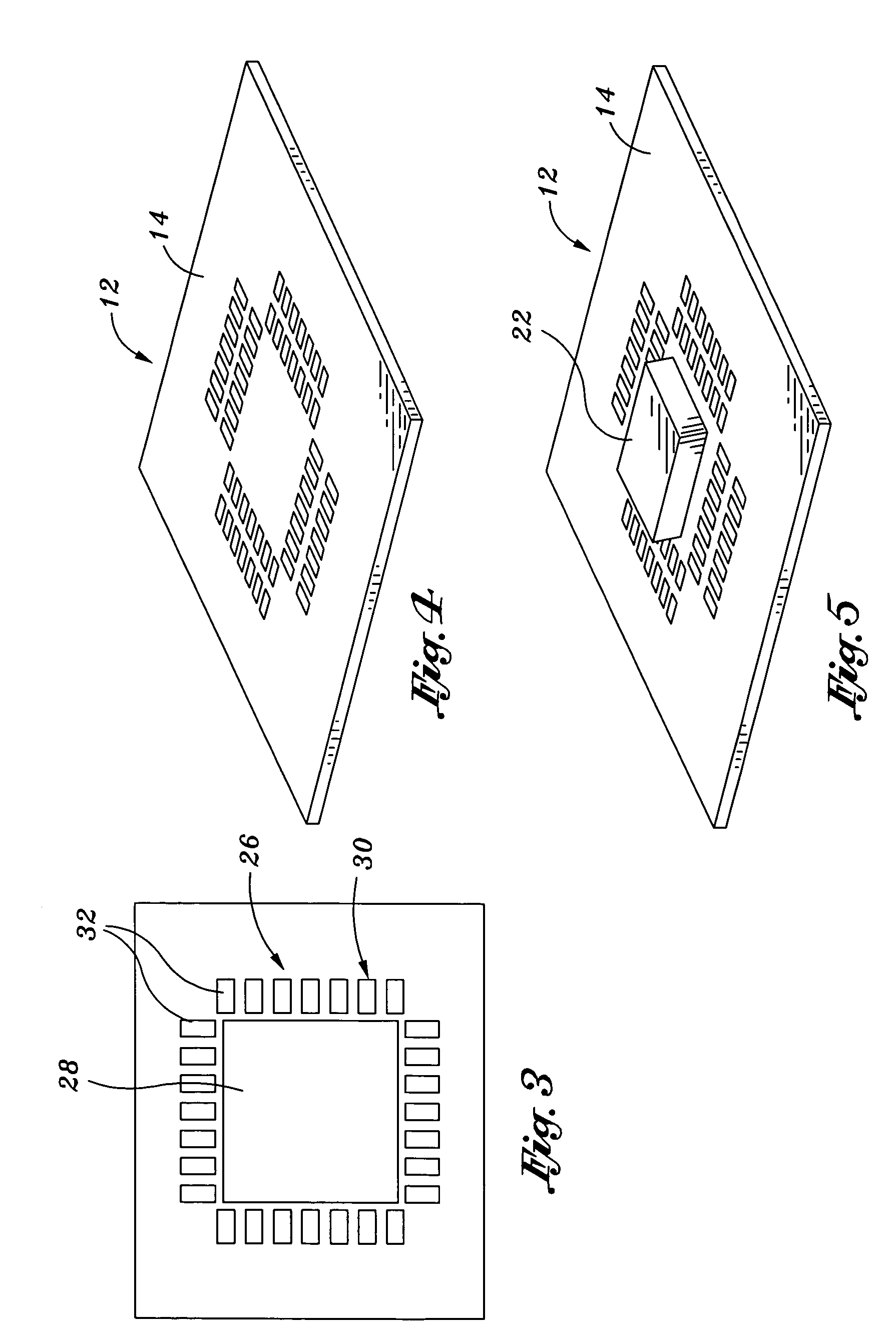
[0016]Referring now to the drawings wherein the showings are for purposes of illustrating preferred embodiments of the present invention only, and not for purposes of limiting the same, FIG. 1 illustrates an embedded leadframe BGA or LGA semiconductor package 10 constructed in accordance with a first embodiment of the present invention. FIG. 3 provides a top plan view of the completed package 10 of the first embodiment.

[0017]The package 10 includes a laminate substrate 12 which has a generally quadrangular (e.g., square, rectangular) configuration. The substrate 12 defines a generally planar top surface 14 and an opposed, generally planar bottom surface 16. The substrate 12 is formed to include a conductive pattern. The conductive pattern itself comprises a plurality of conductive pads 18 of a first set which are disposed on the top surface 14 in a prescribed pattern or array, and a plurality of conductive pads 20 of a second set which are disposed on the bottom surface 16 in a pres...


PUM


Abstract

A semiconductor package comprising a substrate having opposed top and bottom surfaces and a conductive pattern formed thereon. Disposed on the top surface of the substrate is a semiconductor die which is electrically connected to the conductive pattern. Also disposed on the top surface of the substrate is a leadframe which is electrically connected to the conductive pattern as well. A package body encapsulates the semiconductor die and partially encapsulates the leadframe such that a portion of the leadframe is exposed in one exterior surface of the package body, thus allowing a second semiconductor package to be stacked upon and electrically connected to the semiconductor package.

Description

CROSS-REFERENCE TO RELATED APPLICATIONS[0001]Not ApplicableSTATEMENT RE: FEDERALLY SPONSORED RESEARCH / DEVELOPMENT[0002]Not ApplicableBACKGROUND OF THE INVENTION[0003]The present invention relates generally to integrated circuit packaging and, more particularly, to a ball grid array (BGA) or lan grid array (LGA) semiconductor package including an embedded leadframe for allowing the vertical stacking of an LGA or leadframe package thereupon.[0004]A staple component of the electronics industry is a ball grid array (BGA) semiconductor package. BGA packages typically comprise a substrate having a plurality of array-arranged solder balls on the bottom surface thereof. The solder balls act as I / O (input / output) connections for a semiconductor die which is attached to the opposite, top surface of the substrate. In this regard, the substrate is typically provided with a conductive pattern (e.g., pads, traces, vias, etc.), with the semiconductor die being electrically connected to the conduct...

Claims


Application Information

Patent Timeline
Patent Type & Authority Patents(United States)
IPC IPC(8): H01L23/02
CPCH01L23/3128H01L25/105H01L2224/16225H01L2224/48091H01L2224/48227H01L2225/1041H01L2924/15311H01L2225/1023H01L24/48H01L2924/00014H01L2924/14H01L2924/181H01L2924/00H01L2924/00012H01L2224/45099H01L2224/45015H01L2924/207
Inventor SHERIDAN, RICHARD PETERHUEMOELLER, RONALD PATRICKHINER, DAVID JONRUSLI, SUKIANTO
Owner AMKOR TECH SINGAPORE HLDG PTE LTD
Why Eureka
Try Eureka