
Staggered ribs on process chamber to reduce thermal effects

a technology of process chamber and ribs, which is applied in the direction of crystal growth process, chemically reactive gas, coating, etc., can solve the problems of reducing the quality of films that may be grown there, and affecting the uniformity of temperature distribution,

Active Publication Date: 2006-09-19
ASM IP HLDG BV
View PDF10 Cites 255 Cited by
  • Summary
  • Abstract
  • Description
  • Claims
  • Application Information

AI Technical Summary

Benefits of technology

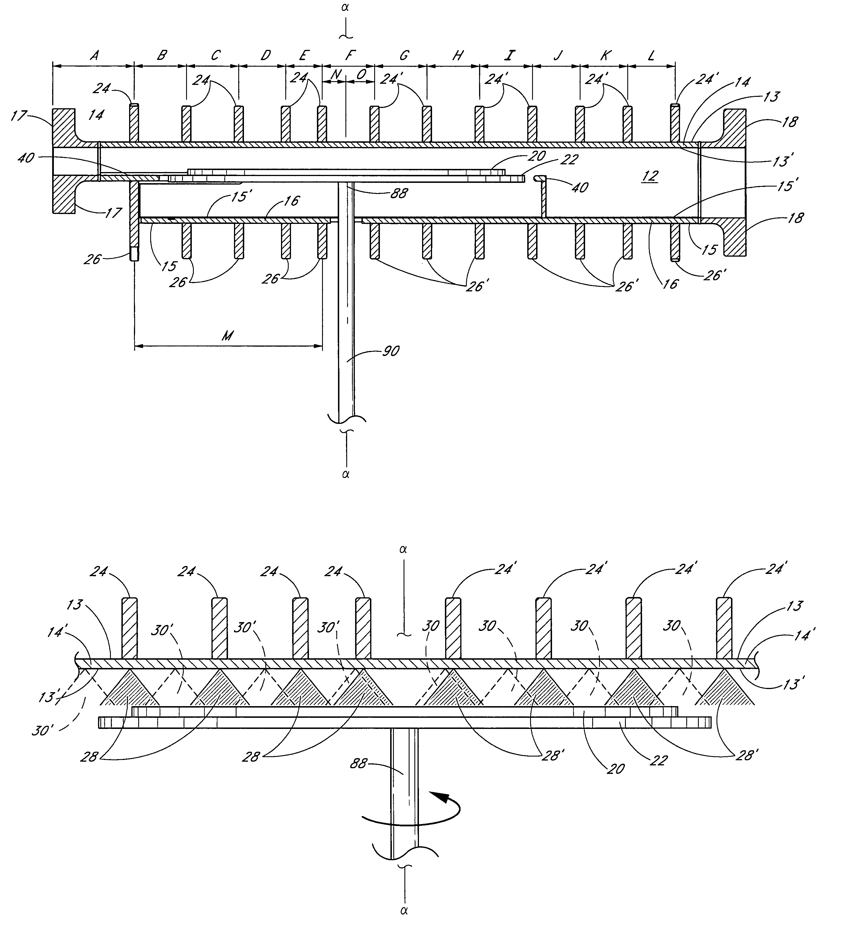
This configuration ensures more uniform radiant energy distribution across the wafer surface, reducing temperature non-uniformities and enhancing the quality of films grown during semiconductor processing.

Problems solved by technology

One disadvantage of such a design is that even though quartz is substantially transparent to the radiant lamp energy, the ribs sections present a region of much thicker quartz, and thus the ribs locally absorb more lamp energy and attenuate the lamp energy delivered to the wafer.
Such non-uniformity of temperature on the wafer surface reduces the quality of the films that may be grown thereon, particularly for process conditions that are temperature-sensitive.
It has been found, however, that if the ribs positioned forward of the wafer center (i.e., the axis of rotation of the wafer) are located at approximately the same distance from the wafer center as are the ribs positioned rearward of the wafer center, temperature uniformity suffers even with rotation.
Specifically, forward and rearward ribs positioned at relatively similar distances from the wafer center cause a combined shadowing effect on the surface of the rotating wafer which can result in temperature distributions that are more non-uniform than can otherwise be achieved.

Method used


Image

  • Staggered ribs on process chamber to reduce thermal effects
  • Staggered ribs on process chamber to reduce thermal effects
  • Staggered ribs on process chamber to reduce thermal effects

Examples


Embodiment Construction

[0018]Although certain preferred embodiments and examples are disclosed below, it will be understood by those skilled in the art that the invention extends beyond the specifically disclosed embodiments to other alternative embodiments and / or uses of the invention and obvious modifications and equivalents thereof. Thus, it is intended that the scope of the invention herein disclosed should not be limited by the particular disclosed embodiments described below.

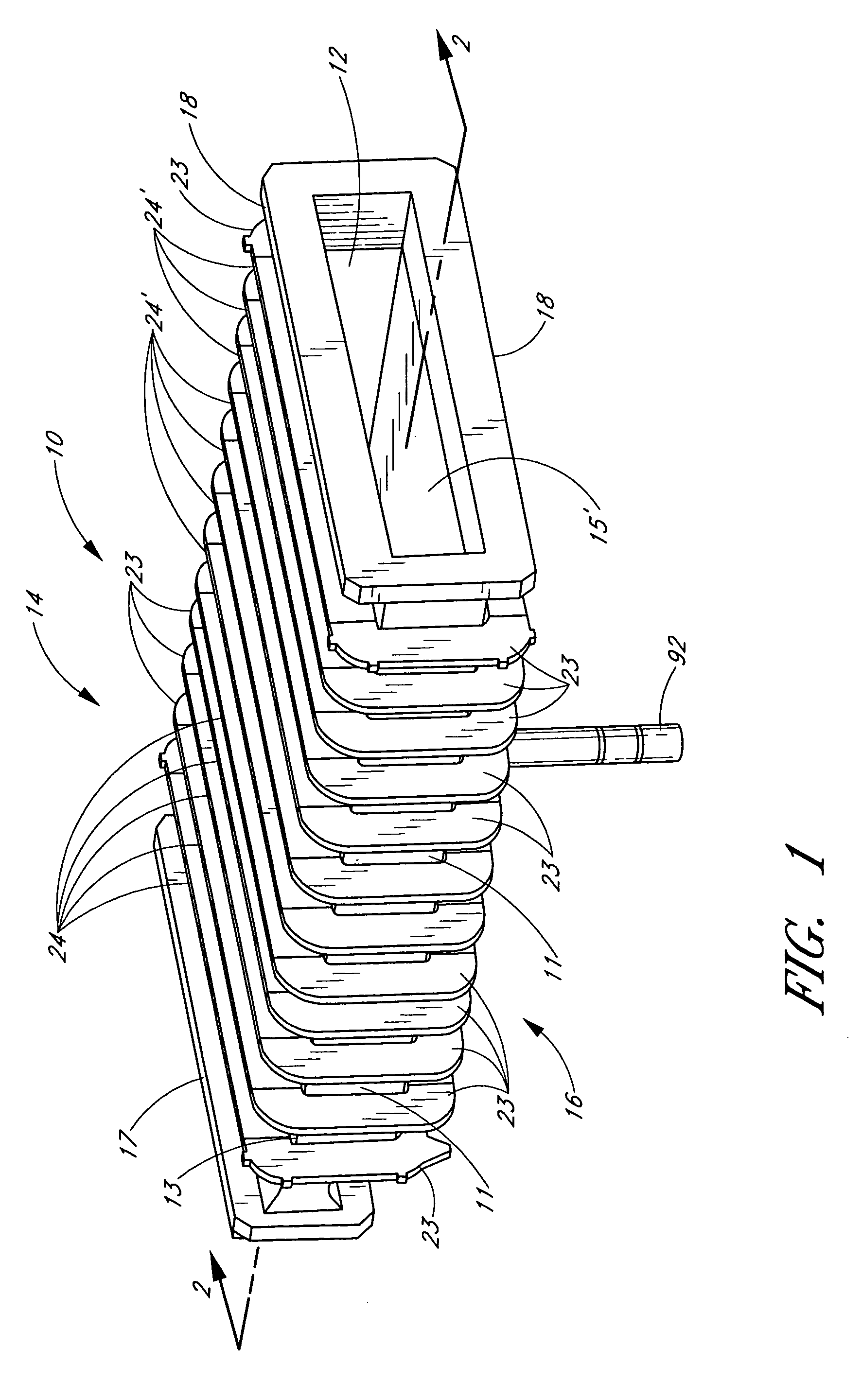
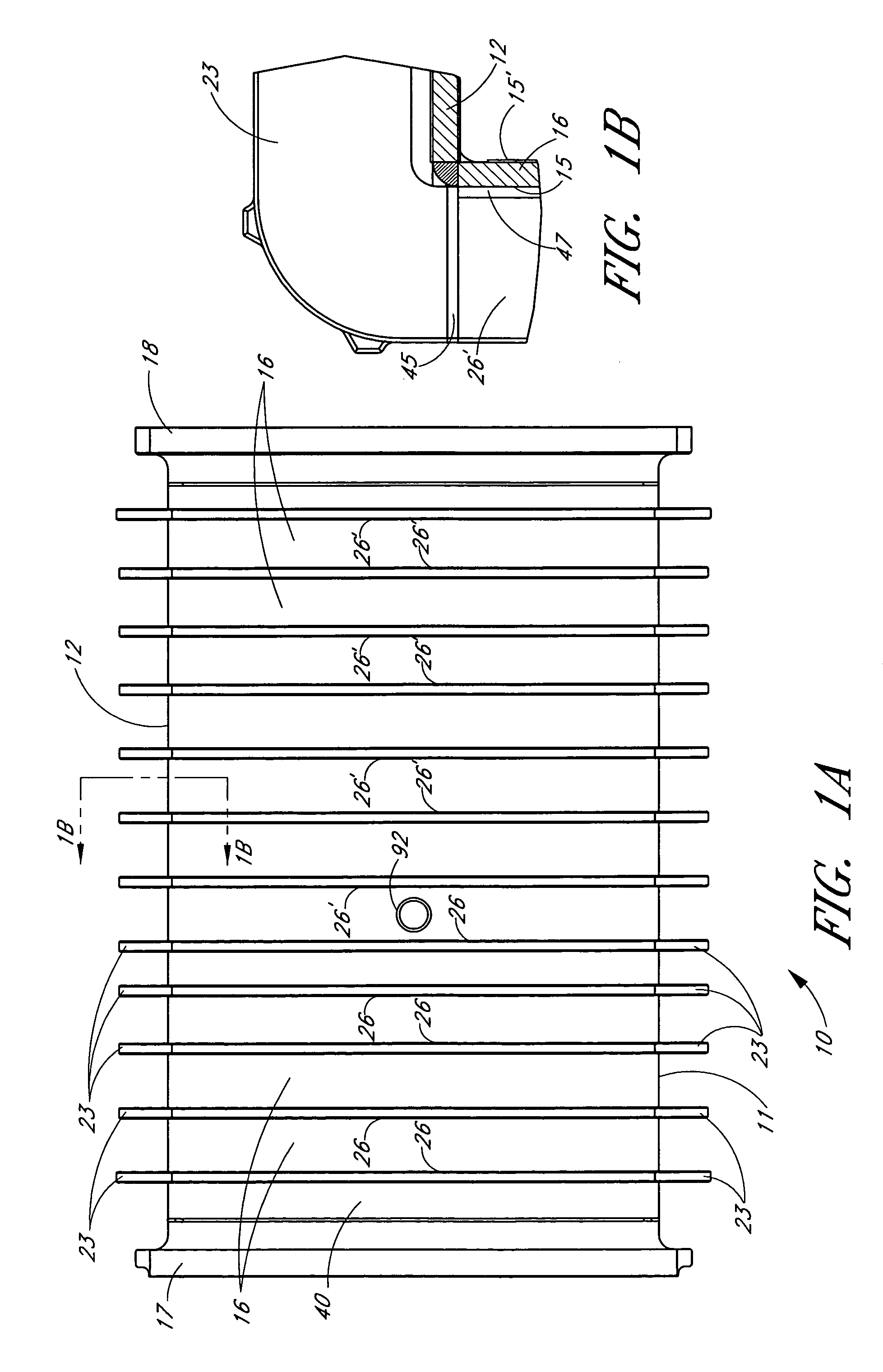
[0019]FIGS. 1–1B illustrate one embodiment of a reactor vessel or chamber 10 for chemical vapor processing. As can be seen, the chamber 10 has an elongated, generally flattened configuration. As best illustrated in FIG. 2, the chamber 10 has an upper wall 14 with an outer surface 13 and an inner surface 13′, and a lower wall 16 with an outer surface 15 and an inner surface 15′. The walls 14, 16 are connected by vertically short side walls 11 and 12. The walls 11, 12, 14, 16 are joined by an upstream inlet flange 17 and a downstr...


PUM

PropertyMeasurementUnit
heightaaaaaaaaaa
widthaaaaaaaaaa
widthaaaaaaaaaa

Abstract

A semiconductor processing chamber having a plurality of ribs on an exterior surface of the chamber is provided. The ribs are positioned relative to the chamber such that shadows cast into the chamber by the ribs are offset from one another, thus more uniformly distributing radiant energy entering the chamber. In one embodiment, the ribs are positioned on the exterior surface of the chamber so that they have dissimilar radial distances from a center of the chamber. When a substrate rotates within the chamber, shadows produced by the ribs on a first side of the chamber fall substantially between secondary shadows produced by the ribs on a second side of the chamber. Likewise, shadows produced by the ribs on the second side of the chamber fall substantially between the secondary shadows produced by the ribs on the first side of the chamber.

Description

BACKGROUND OF THE INVENTION[0001]1. Field of the Invention[0002]This invention relates generally to semiconductor processing chambers, and relates more particularly in one embodiment to the positioning of ribs on exterior surfaces of a process chamber to reduce thermal effects within the process chamber.[0003]2. Description of the Related Art[0004]Process chambers for thermally processing semiconductor wafers typically are made of quartz (vitreous silica) or similar material because quartz is substantially transparent to radiant energy. Radiant heaters may be positioned adjacent the exterior of the chamber, and a wafer being processed in the chamber can be heated to elevated temperatures without having the chamber walls heated to the same level. Furthermore, quartz is desirable because it can withstand very high temperatures, and its inert characteristics enable it to withstand degradation by various processing gases.[0005]For applications in which the pressure within a quartz chamb...

Claims


Application Information

Patent Timeline
Patent Type & Authority Patents(United States)
IPC IPC(8): C23C16/46C23C16/458H01L21/306C23C16/00C23C16/44C23C16/48C30B25/08C30B31/10
CPCC23C16/44C30B31/10C30B25/08C23C16/481
Inventor WOOD, ERIC R.
Owner ASM IP HLDG BV
Learn More