Plating system for semiconductor materials

Inactive Publication Date: 2006-08-08
APPLIED MATERIALS INC
View PDF22 Cites 31 Cited by
  • Summary
  • Abstract
  • Description
  • Claims
  • Application Information

AI Technical Summary

Problems solved by technology

The cost of manufacturing and maintaining these clean rooms is very expensive, and therefore any progress that can be made towards reducing the size of the semiconductor manufacturing machines will allow for smaller clean rooms.
Any unevenness in application of material to the wafer will result in semiconductor chips which are not of sufficient quality and must be destroyed.
The electroplating process requires the handling of a large volume of liquid which necessarily implies the use of pumps, piping, and other components, all of which take up valuable space in a clean room environment.

Method used


Image

  • Plating system for semiconductor materials
  • Plating system for semiconductor materials
  • Plating system for semiconductor materials

Examples


Embodiment Construction

[0040]This disclosure of the invention is submitted in furtherance of the constitutional purposes of the U.S. Patent Laws “to promote the progress of science and useful arts” (Article 1, Section 8).

[0041]

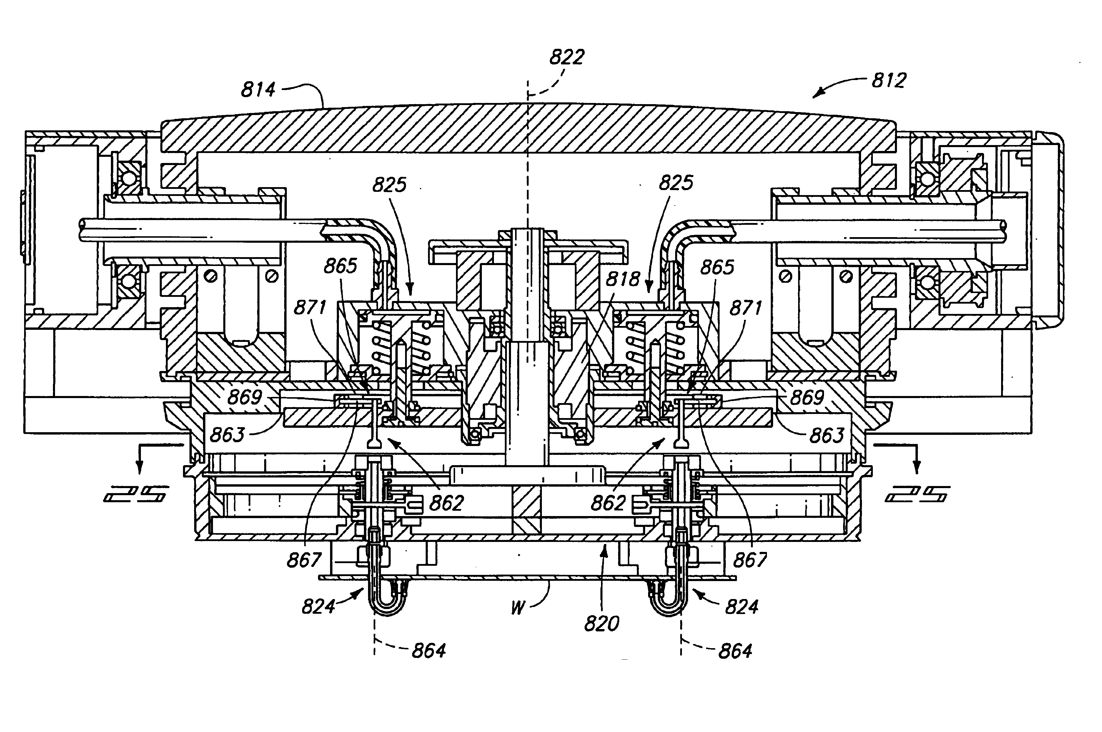
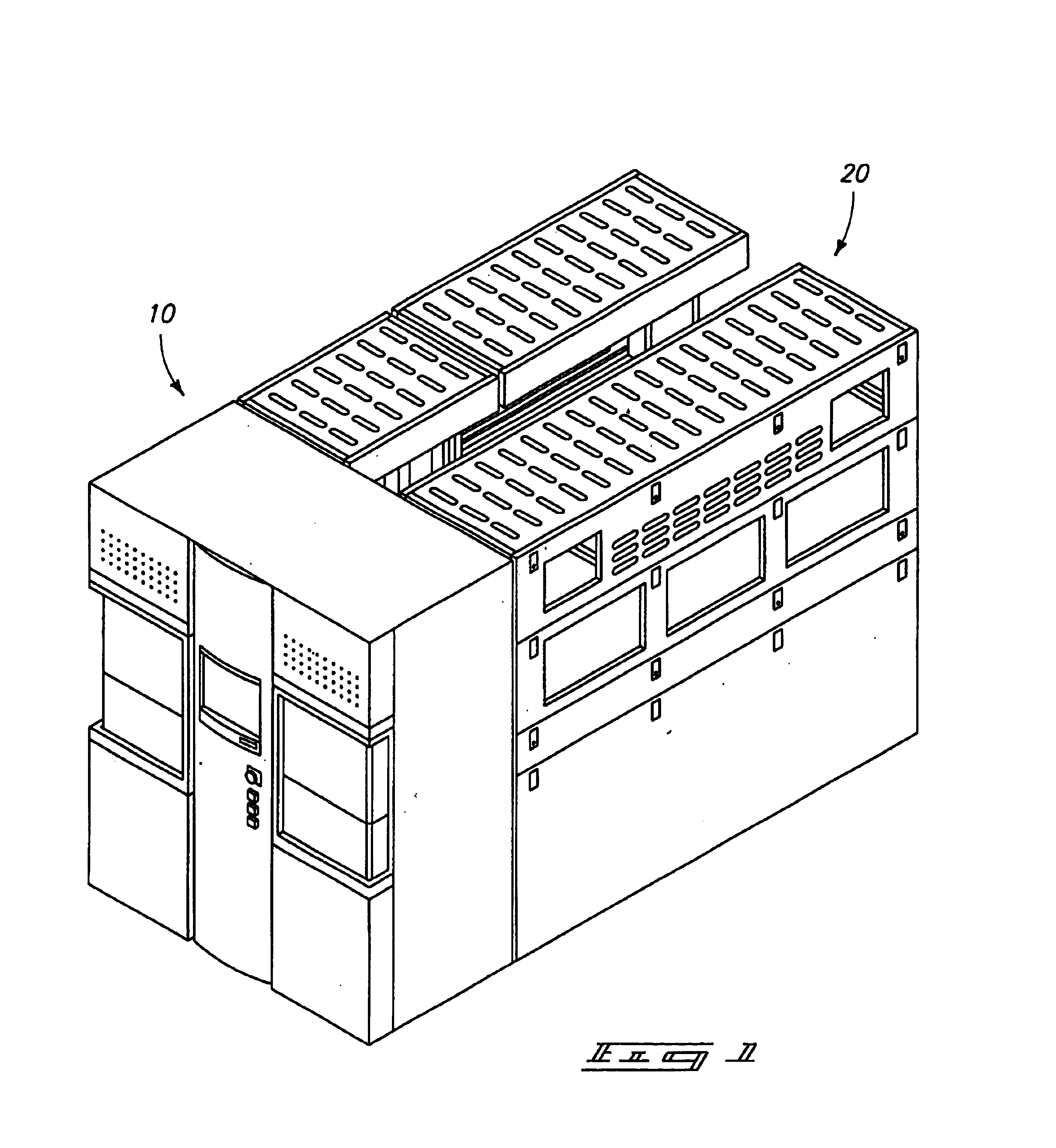
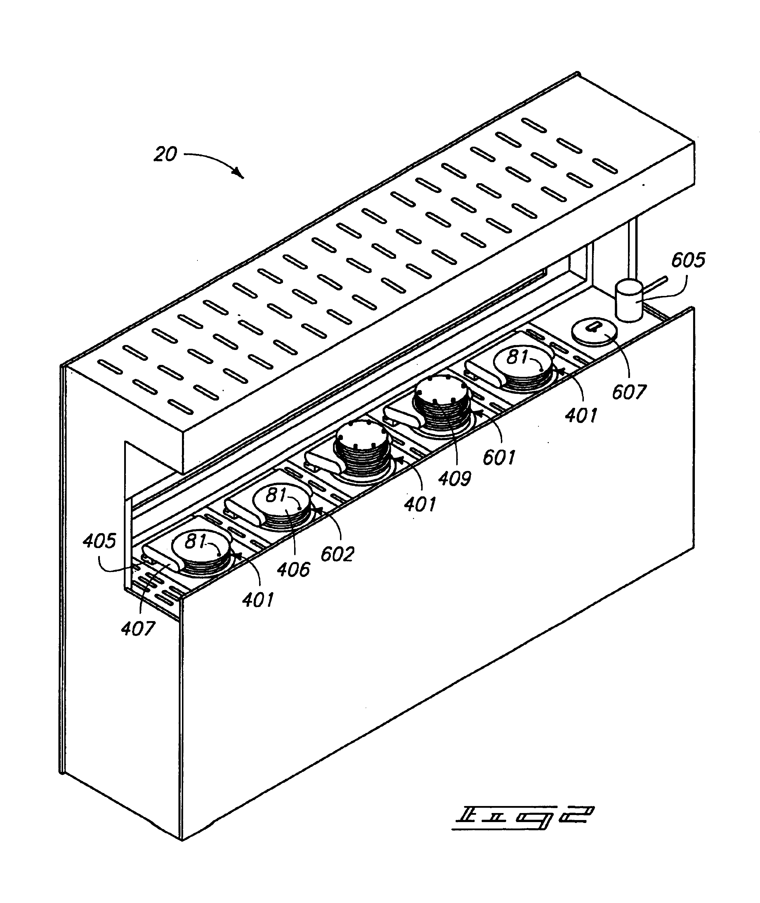
TABLE 1Listing of Subsections of Detailed Description andPertinent Items with Reference Numerals and Page NumbersWorkpiece Processing Station10semiconductor workpiece process tool1010electroplating module 2010workpiece support 40110processing head 40610operator arm 40710operator base 40510fingers 40910beam emitter 8111plating chamber assemblies 60311process fluid reservoir 60411immersible pump 60511module frame or chassis 60612pump discharge filter 60712outer reservoir wall 60812inner reservoir wall 60912reservoir safety volume 61112inner vessel 61212reservoir overflow opening 61012heat exchanger 61313exchanger inlet 61413exchanger outlet 61513Bowl Assembly13reservoir top 61813process bowl or plating chamber 61613bowl side 61713bowl bottom 61913cup assembly 62013fluid cup 62113cup s...


PUM

PropertyMeasurementUnit
Lengthaaaaaaaaaa
Flow rateaaaaaaaaaa
Diameteraaaaaaaaaa

Abstract

A workpiece processing station is disclosed. The workpiece processing station has particular applicability in an electroplating process for semiconductor wafers. The apparatus includes a work processing bowl having an outer bowl and an inner cup positioned at a location slightly below the upper rim of the bowl. An annular space is provided between the sides of the processing bowl and the fluid cup. Fluid is provided to the fluid cup through an opening in the bottom of the fluid cup. The fluid overflows the fluid cup and drains down the open annular space between the process bowl and the fluid cup and passes through the opening in the bottom of the process bowl and into a fluid reservoir. A reservoir is preferably used as both the supply and the return for the process fluid. The apparatus further includes filters disposed within the bottom of each fluid cup between the bottom of the fluid cup and the process fluid inlet line such that the process fluid must flow upward through the filter before entering the upper portion of the fluid cup. In the preferred embodiment, the workpiece processing station includes a plurality of the process bowl assemblies all having a common reservoir in which process fluid may drain. The invention also includes the method of flowing process fluid into a process vessel such that it overflows and returns to a common fluid return reservoir during the semiconductor manufacturing process.

Description

TECHNICAL FIELD[0001]This invention pertains to semiconductor manufacturing machines in general and in particular to semiconductor processing stations and more particularly semiconductor electroplating work stations.BACKGROUND OF THE INVENTION[0002]In the manufacture of semiconductors and microchips, one method of manufacture is to use a large wafer of semiconductor material such as silicon dioxide and manufacture many microchips out of a single wafer. The wafer is then separated into the individual microchips. Manufacturing by using the single wafer has the advantage of increasing throughput in the semiconductor manufacturing process. Obviously the larger the wafer that can be used the more efficiency is obtained and the higher the throughput will be. However, since microchips contain many circuits of minuscule dimensions, the manufacturing process must be very precise and accurate to ensure that all microchips manufactured out of a single wafer are of the same quality.[0003]One st...

Claims


Application Information

Patent Timeline
IPC IPC(8): C25D17/00C25D7/12H01L21/00
CPCC25D7/12C25D17/001H01L21/6715Y10S134/902
Inventor SCHMIDT, WAYNE J.BERNER, ROBERT W.WOODRUFF, DANIEL J.
Owner APPLIED MATERIALS INC
Why Eureka
Try Eureka