Optical materials in packaging micromirror devices
- Summary
- Abstract
- Description
- Claims
- Application Information
AI Technical Summary
Problems solved by technology
Method used
Image
Examples
Embodiment Construction
[0018]Turning to the drawings, the present invention is illustrated as being implemented in a suitable packaging process for micromirror array devices. The following description is based on embodiments of the invention and should not be interpreted as limitations of the invention with regard to alternative embodiments that are not explicitly described herein.
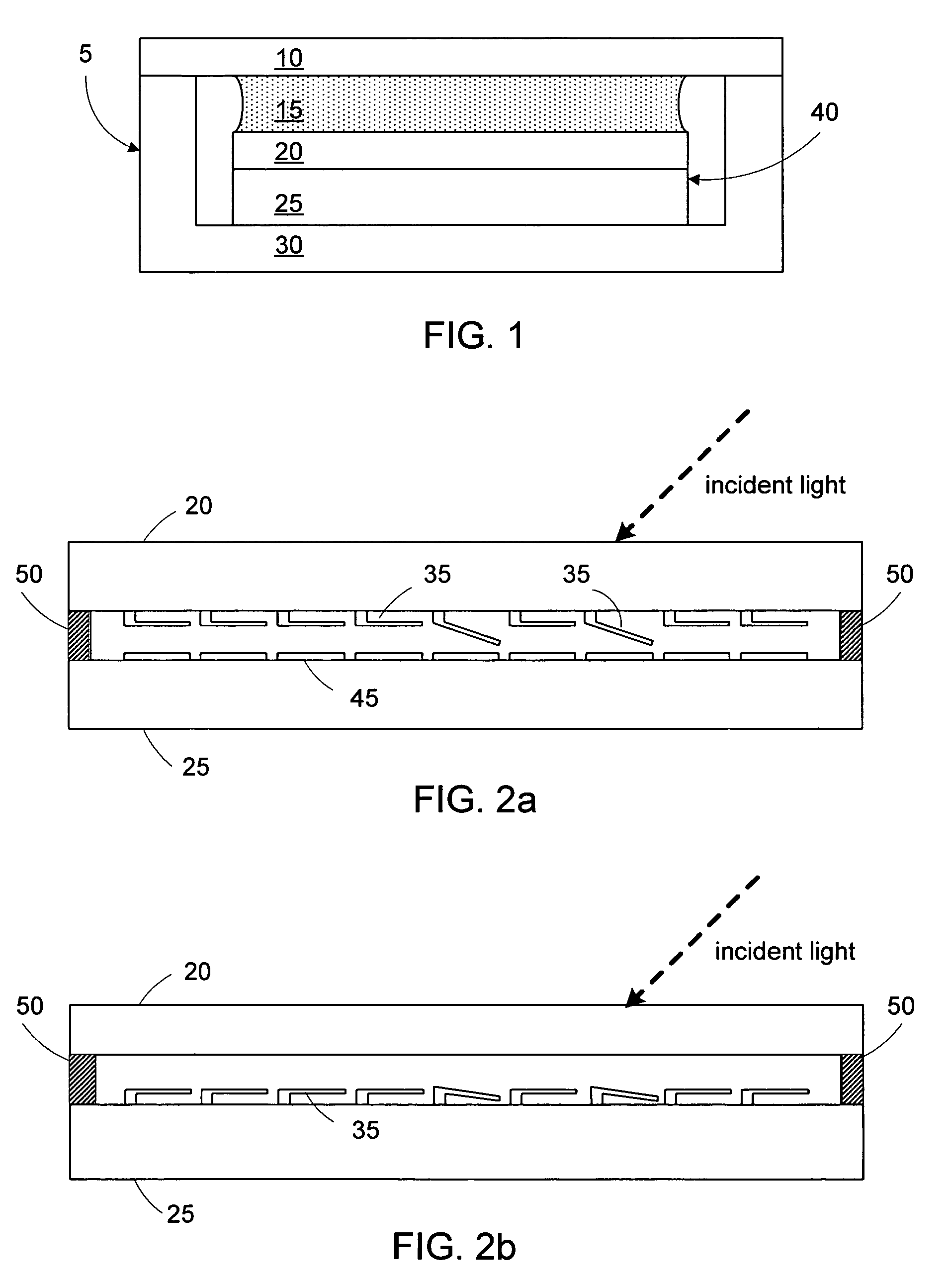
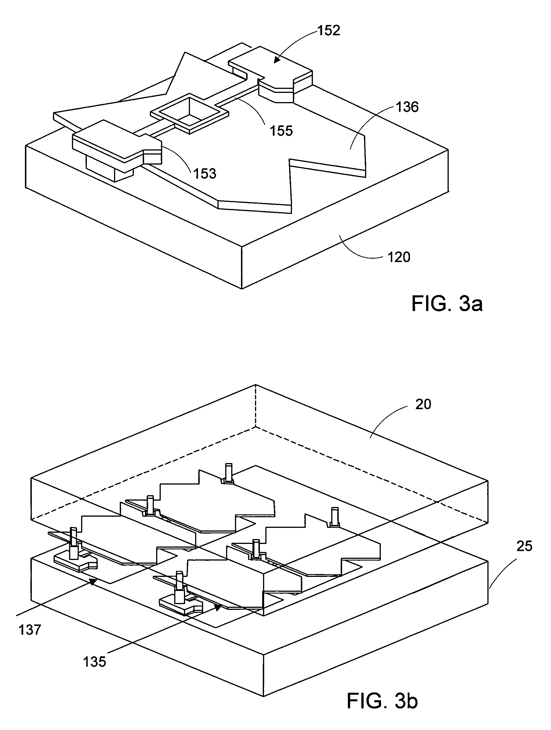
[0019]Referring to FIG. 1, micromirror array device 40 comprises glass substrate 20, semiconductor substrate 25 and a plurality of micromirrors for modulating incident light. Depending upon specific design, the plurality of micromirrors can be formed on the glass substrate or the semiconductor substrate, as shown respectively in FIG. 2a and FIG. 2b. Though the methods, materials and mirror structures in FIG. 2a and FIG. 2b can be very different, the package needs, including the need to reduce reflection, can be similar. Specifically, referring to FIG. 2a, the micromirrors (e.g. micromirror 35) are formed on glass substrate 20, s...
PUM
 Abstract
Description
Claims
Application Information
 - R&D
- Intellectual Property
- Life Sciences
- Materials
- Tech Scout
- Unparalleled Data Quality
- Higher Quality Content
- 60% Fewer Hallucinations
Browse by: Latest US Patents, China's latest patents, Technical Efficacy Thesaurus, Application Domain, Technology Topic, Popular Technical Reports.
© 2025 PatSnap. All rights reserved.Legal|Privacy policy|Modern Slavery Act Transparency Statement|Sitemap|About US| Contact US: help@patsnap.com


