Compensation circuit for current control oscillator
a current control oscillator and compensating circuit technology, applied in the direction of pulse automatic control, pulse generation by logic circuits, pulse technique, etc., can solve the problems of undesirable frequency output and problems of foregoing setup, and achieve the effect of eliminating the parasite effect and improving the parasite load phenomenon
- Summary
- Abstract
- Description
- Claims
- Application Information
AI Technical Summary
Benefits of technology
Problems solved by technology
Method used
Image
Examples
first embodiment
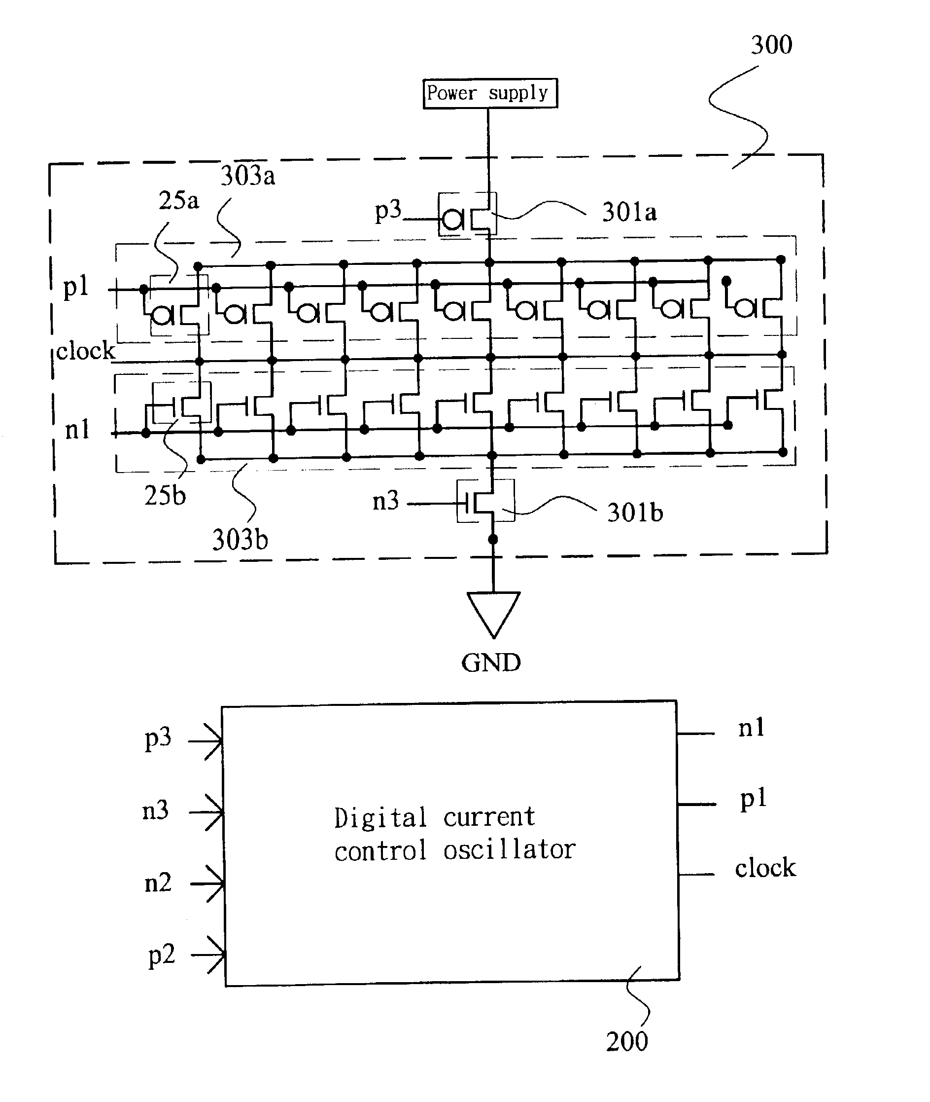
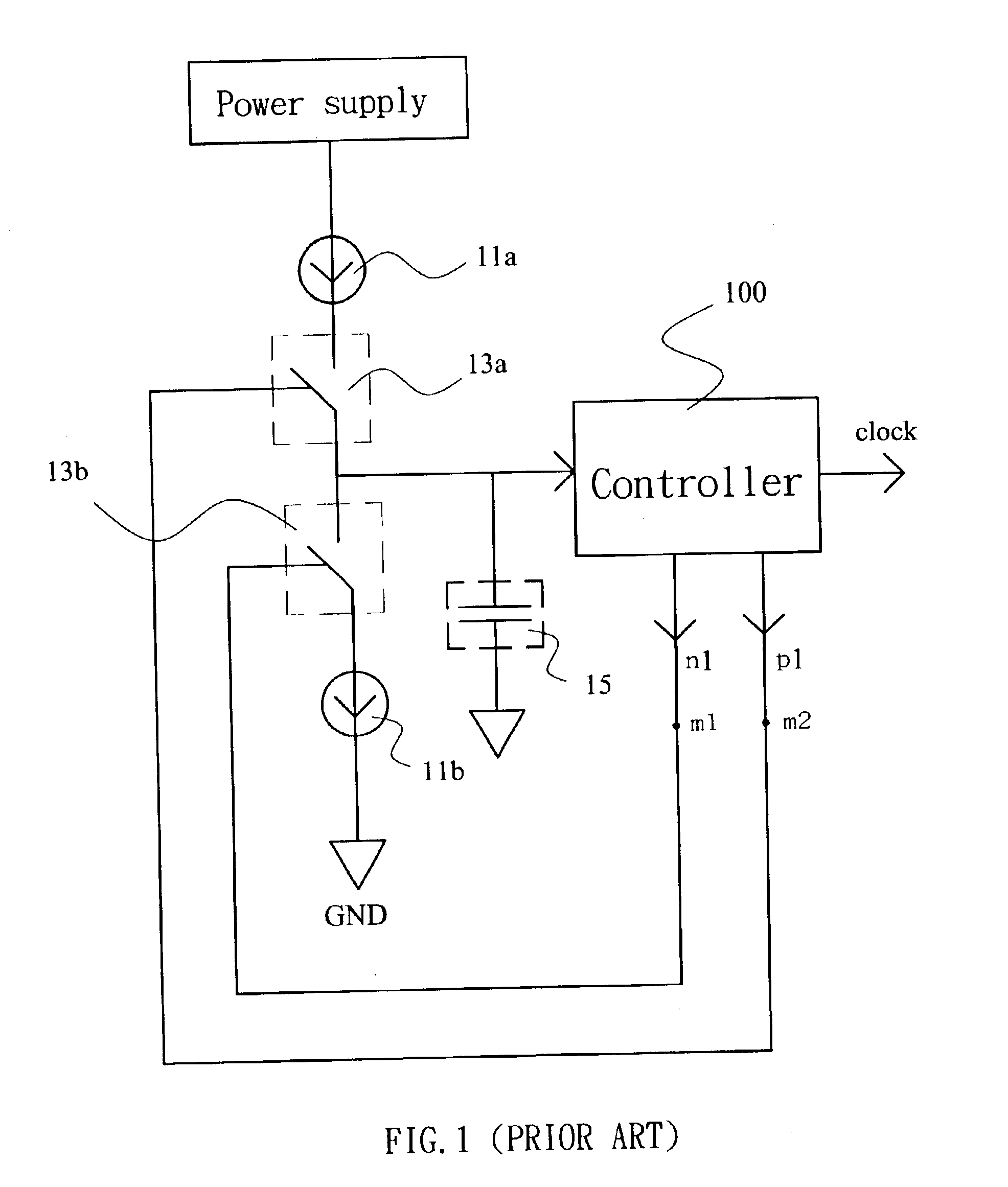
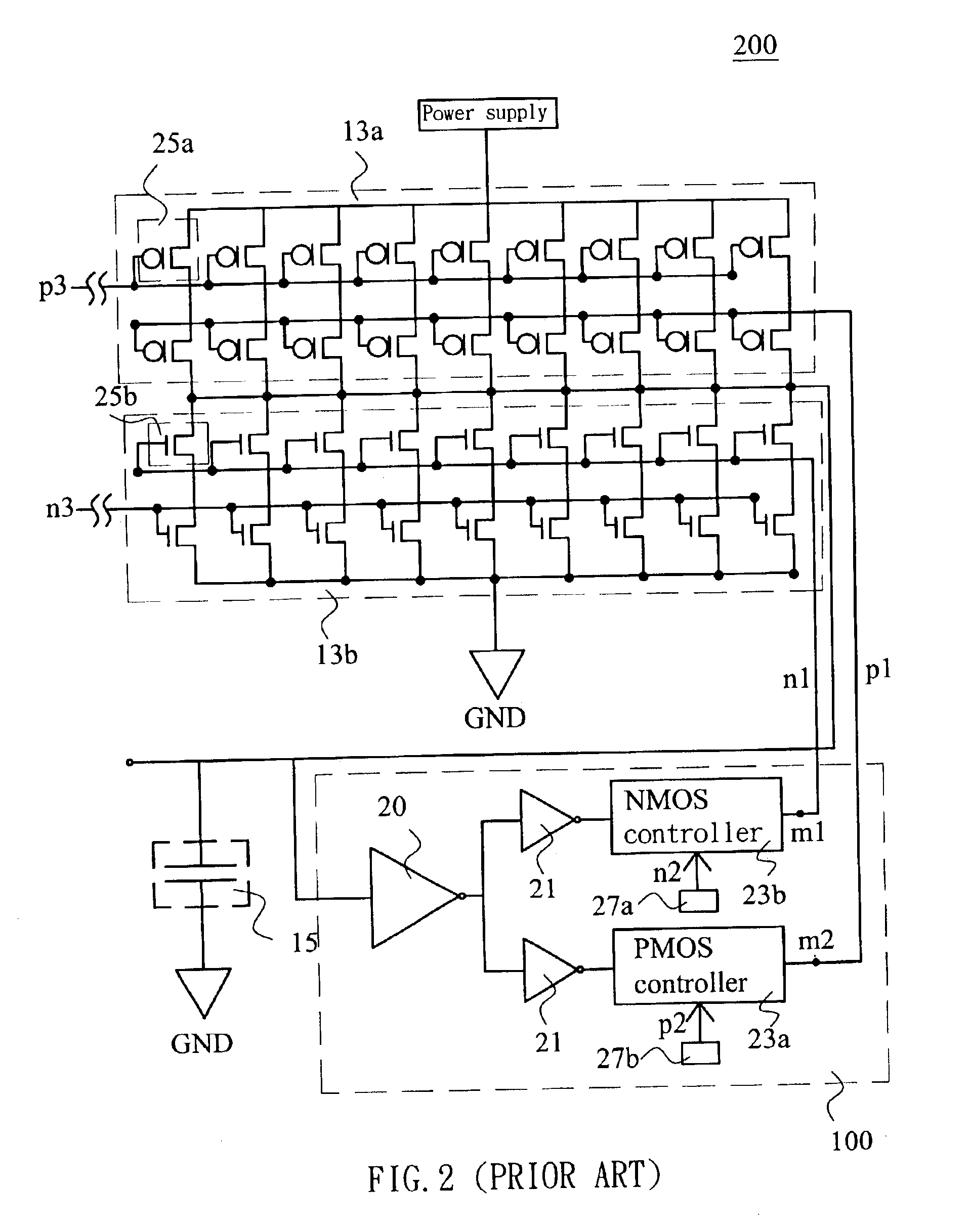
Refer to FIG. 3 for the digital current control oscillator coupled with the compensation circuit according to the invention. A conventional digital current control oscillator 200 has a P bus p1 and N bus n1 connecting to a compensation circuit 300. The compensation circuit 300 includes a P compensation circuit 303a which has one end connecting to a P connection end p3 of the digital current control oscillator 200 through a P passage switch 301a, and a N compensation circuit 303b which has one end connecting to a N connection end n3 of the digital current control oscillator 200 through a N passage switch 301b. The compensation circuit 300 consists of a P compensation circuit 303a and a N compensation circuit 303b that are formed by connecting a plurality of P transistors 25a and N transistors 25b in series. As the digital current control oscillator 200 will occur parasite load phenomenon due to different number of charge and discharge transistor switches, the compensation circuit 300...
second embodiment
Referring to FIG. 4 for the digital current control oscillator coupled with the compensation circuit according to the invention. In this embodiment the number of P transistors 25a and the N transistors 25b in the compensation circuit 300 is constant. The P transistors 25a in the charge transistor switch 13a follow the control of the PMOS controller 23a to adjust the transistor switch number connecting to the P bus. The P passage switch 301a is ON when the equivalent load capacitor 15 is charging, and is OFF while discharging. On the other hand, The N transistors 25b in the discharge transistor switch 13b follow the control of the NMOS controller 23b to adjust the transistor switch number connecting to the N bus. The N passage switch 301b is ON when the equivalent load capacitor 15 is discharging, and is OFF while charging. In this embodiment, the characteristics of the transistors (MOS) contained in the charge transistor switch 13a, discharge transistor switch 13b, P compensation ci...
PUM
 Abstract
Description
Claims
Application Information
 - R&D Engineer
- R&D Manager
- IP Professional
- Industry Leading Data Capabilities
- Powerful AI technology
- Patent DNA Extraction
Browse by: Latest US Patents, China's latest patents, Technical Efficacy Thesaurus, Application Domain, Technology Topic, Popular Technical Reports.
© 2024 PatSnap. All rights reserved.Legal|Privacy policy|Modern Slavery Act Transparency Statement|Sitemap|About US| Contact US: help@patsnap.com


