
System and method of transferring dies using an adhesive surface

a technology of adhesive surface and die, applied in the field of electronic device assembly, can solve the problems of limited throughput volume, limited placement accuracy of pick and place techniques, and drawbacks of limiting throughput volum

Inactive Publication Date: 2005-02-01
SYMBOL TECH INC
View PDF4 Cites 112 Cited by
  • Summary
  • Abstract
  • Description
  • Claims
  • Application Information

AI Technical Summary

Problems solved by technology

Pick and place techniques involve complex robotic components and control systems that handle only one die at a time.
This has a drawback of limiting throughput volume.
Furthermore, pick and place techniques have limited placement accuracy, and have a minimum die size requirement.

Method used


Image

  • System and method of transferring dies using an adhesive surface
  • System and method of transferring dies using an adhesive surface
  • System and method of transferring dies using an adhesive surface

Examples


Embodiment Construction

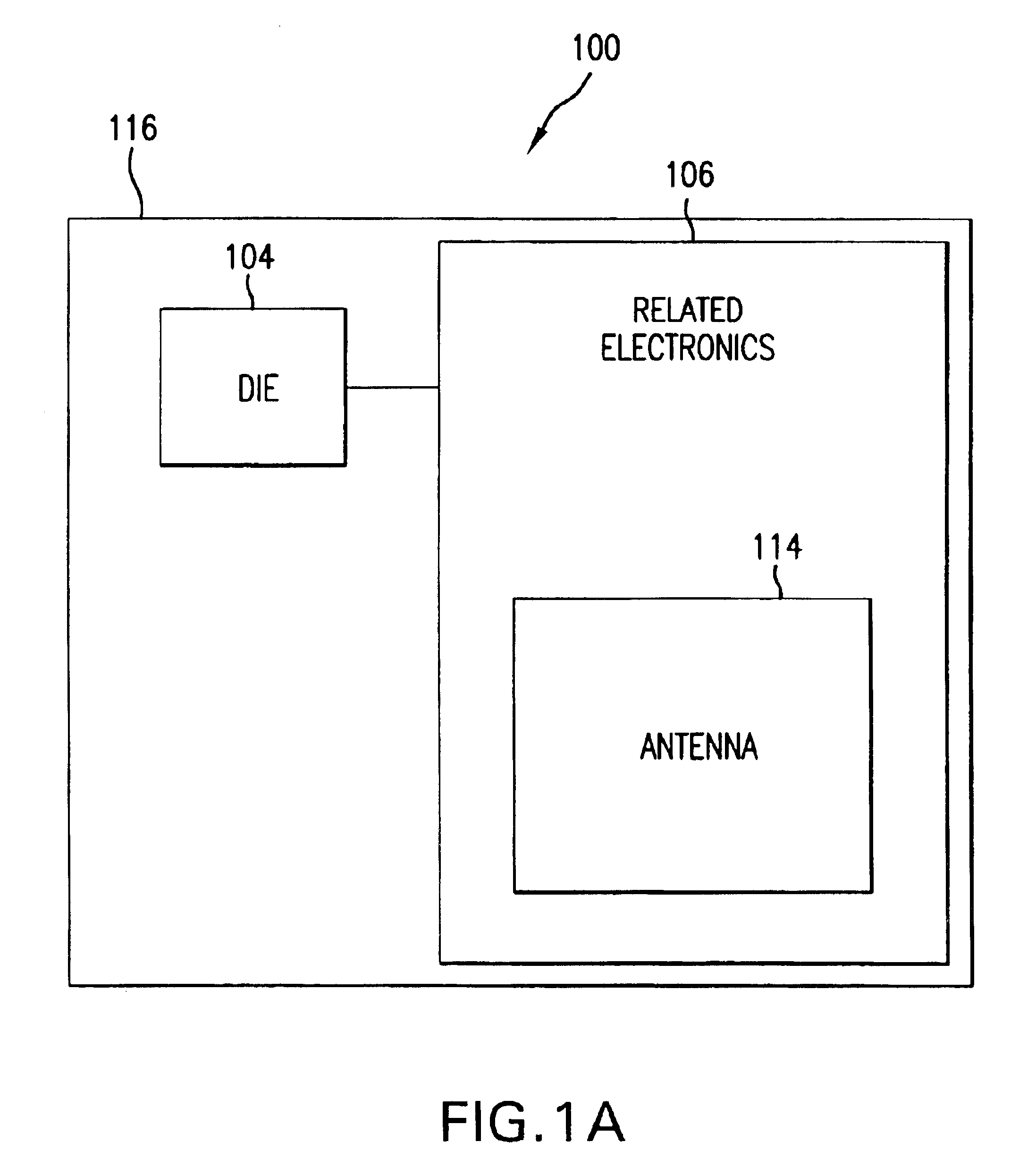
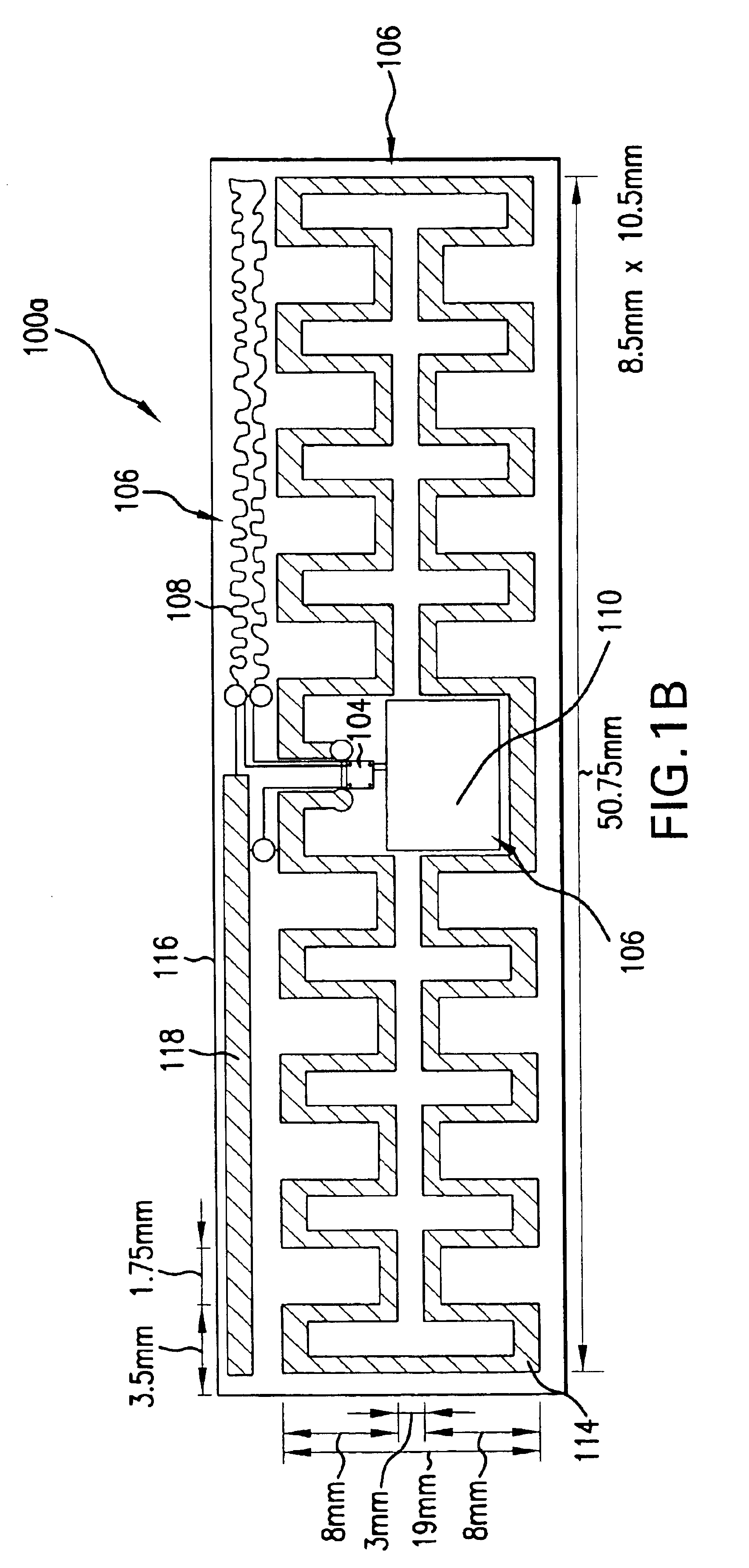
The present invention provides improved processes and systems for assembling electronic devices, including RFID tags. The present invention provides improvements over current processes. Conventional techniques include vision-based systems that pick and place dies one at a time onto substrates. The present invention can transfer multiple dies simultaneously. Vision-based systems are limited as far as the size of dies that may be handled, such as being limited to dies larger than 600 microns square. The present invention is applicable to dies 100 microns square and even smaller. Furthermore, yield is poor in conventional systems, where two or more dies may be accidentally picked up at a time, causing losses of additional dies.

The present invention provides an advantage of simplicity. Conventional die transfer tape mechanisms may be used by the present invention. Furthermore, much higher fabrication rates are possible. Current techniques process 5-8 units per hour. The present inventio...


PUM

PropertyMeasurementUnit
thicknessesaaaaaaaaaa
thicknessaaaaaaaaaa
thicknessaaaaaaaaaa

Abstract

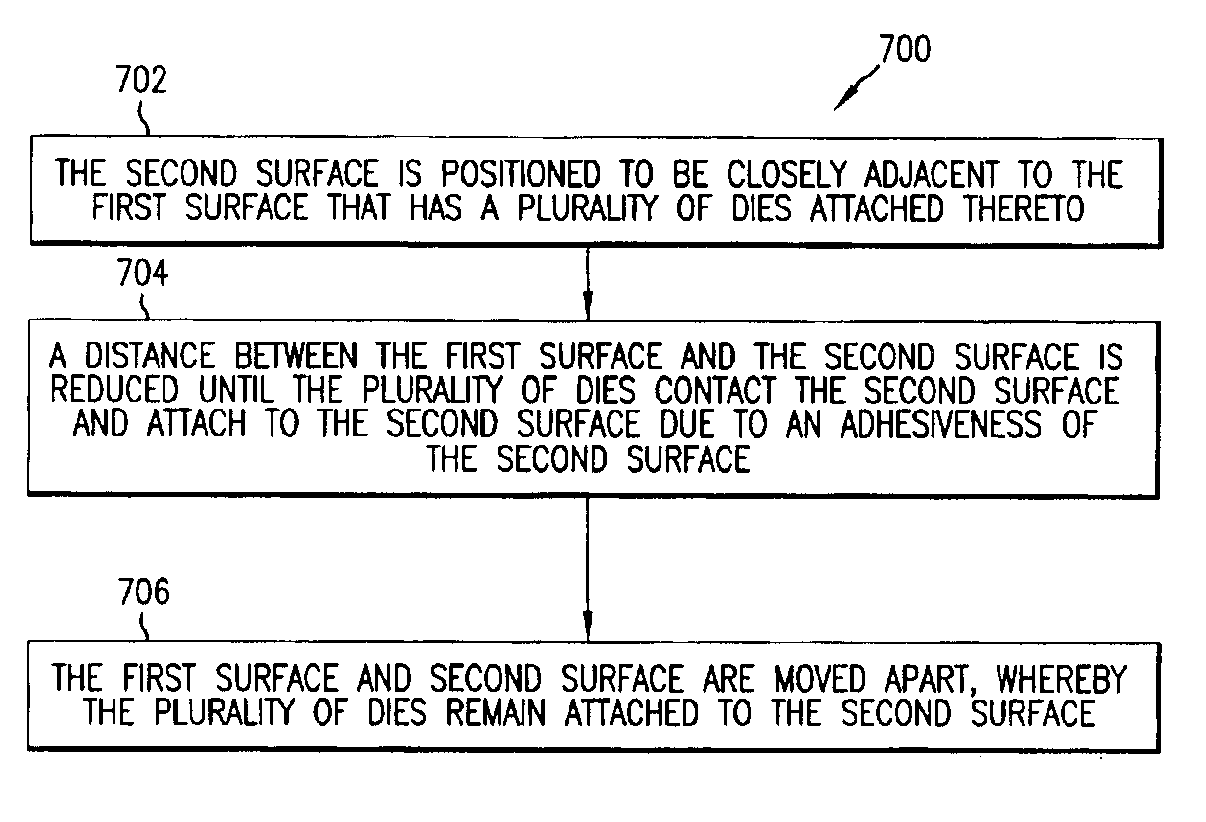
A method and system for transferring a plurality of integrated circuit dies from a first surface to a second surface is described. The second surface is positioned to be closely adjacent to the first surface that has a plurality of dies attached thereto. A distance is reduced between the first surface and the second surface until the plurality of dies contact the second surface and attach to the second surface due to an adhesiveness of the second surface. The first surface and second surface are moved apart. The plurality of dies remain attached to the second surface.

Description

BACKGROUND OF THE INVENTION1. Field of the InventionThe present invention relates generally to the assembly of electronic devices. More particularly, the present invention relates to the assembly of radio frequency identification (RFID) tags.2. Related ArtPick and place techniques are often used to assemble electronic devices. Such techniques involve a manipulator, such as a robot arm, to remove integrated circuit (IC) dies from a wafer and place them into a die carrier. The dies are subsequently mounted onto a substrate with other electronic components, such as antennas, capacitors, resistors, and inductors to form an electronic device.Pick and place techniques involve complex robotic components and control systems that handle only one die at a time. This has a drawback of limiting throughput volume. Furthermore, pick and place techniques have limited placement accuracy, and have a minimum die size requirement.One type of electronic device that may be assembled using pick and place...

Claims


Application Information

Patent Timeline
Patent Type & Authority Patents(United States)
IPC IPC(8): H01L21/02G06K19/077H01L21/56H01L21/68H01L21/67H01L23/498H01L23/48
CPCG06K19/07745G06K19/07749G06K19/0775G06K19/07758H01L21/56H01L21/6835H01L23/49855H01L24/96G06K19/07718B29C33/06Y10T29/49885H01L2221/68354H01L2224/16H01L2224/83191H01L2924/01013H01L2924/01027H01L2924/01033H01L2924/01047H01L2924/01077H01L2924/01079H01L2924/01082H01L2924/09701H01L2924/14H01L2924/19041H01L2924/19042H01L2924/19043H01L2924/01005H01L2924/01006H01L2224/16225H01L2224/16227H01L2224/81191Y10T29/53039Y10T29/49826Y10T29/53178Y10T29/49155Y10T156/10Y10T29/53191Y10T29/5313Y10T29/4902Y10T29/49016Y10T29/49117Y10T29/53261H01L2924/12042H01L2924/00
Inventor ARNESON, MICHAEL R.BANDY, WILLIAM R.
Owner SYMBOL TECH INC
Learn More