Electro-optic device and electronic apparatus

a technology of optical devices and electronic devices, applied in semiconductor devices, diodes, instruments, etc., can solve the problems of short circuit between wires and easy reduction of yield, and achieve the effect of improving light emission performan

Active Publication Date: 2017-08-10
SEIKO EPSON CORP
View PDF1 Cites 1 Cited by
  • Summary
  • Abstract
  • Description
  • Claims
  • Application Information

AI Technical Summary

Benefits of technology

[0017]According to this application example, an electronic apparatus having a light-emitting element with an improved light emission performance can be provided.

Problems solved by technology

The light-emitting device described in JP-A-2015-76300, however, may develop a short circuit between the peripheral wiring and the electrode (anode) or the like of the pixel portion in the case where the optical path length adjustment layer that covers the peripheral wiring is thin.
More particularly, in the manufacturing process of the above light-emitting device, a minute foreign substance or dust may mix into the optical path length adjustment layer when a film is formed, thereby causing a short circuit to occur between wires.
Such short-circuiting is problematic in that it hinders the light-emitting feature of the light-emitting device, which affects the light-emitting quality of the light-emitting device and leads to reduced yield easily.

Method used


Image

  • Electro-optic device and electronic apparatus
  • Electro-optic device and electronic apparatus
  • Electro-optic device and electronic apparatus

Examples


embodiment 1

Electro-Optic Device

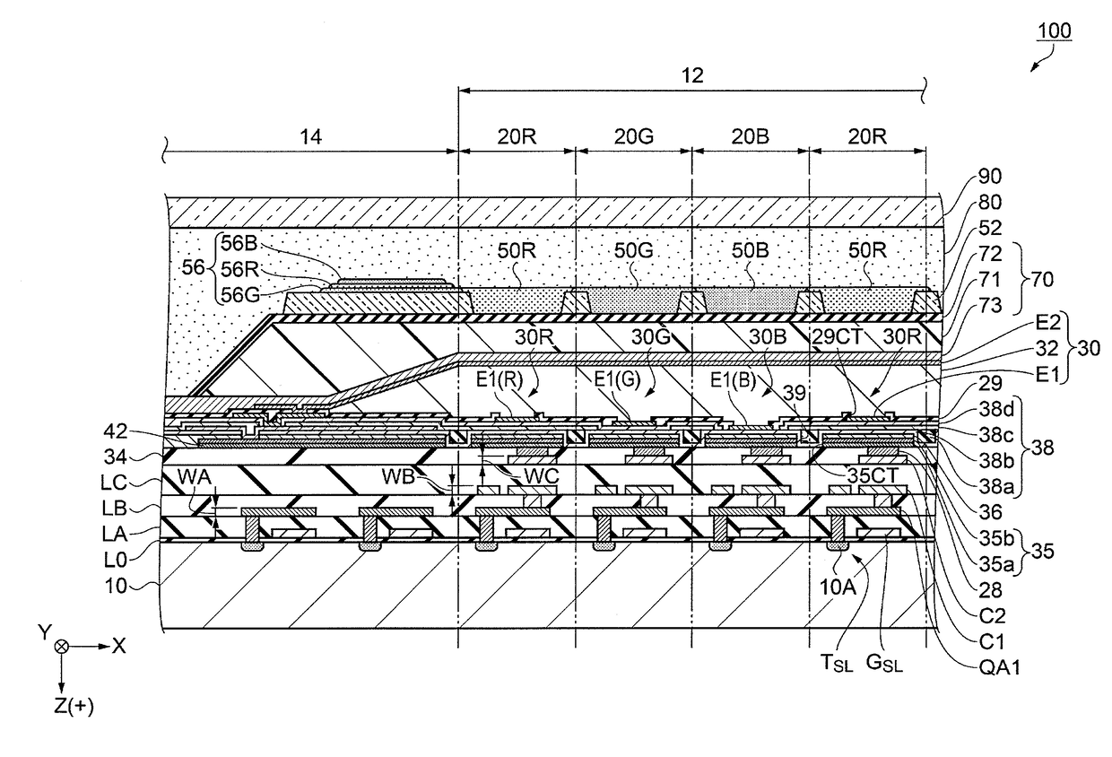
[0026]Referring to FIG. 1, an electro-optic device according to this embodiment is described. In this embodiment, an example of an electro-optic device includes an organic electroluminescent (EL) device. FIG. 1 is a plan view illustrating the structure of an organic EL device according to Embodiment 1 of the invention.

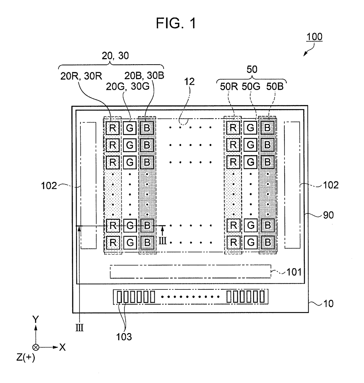
[0027]As illustrated in FIG. 1, an organic EL device 100 in this embodiment has an element substrate 10 and a counter substrate 90. The element substrate 10 and the counter substrate 90, facing each other, are bonded to each other with a filler layer, which is described later.

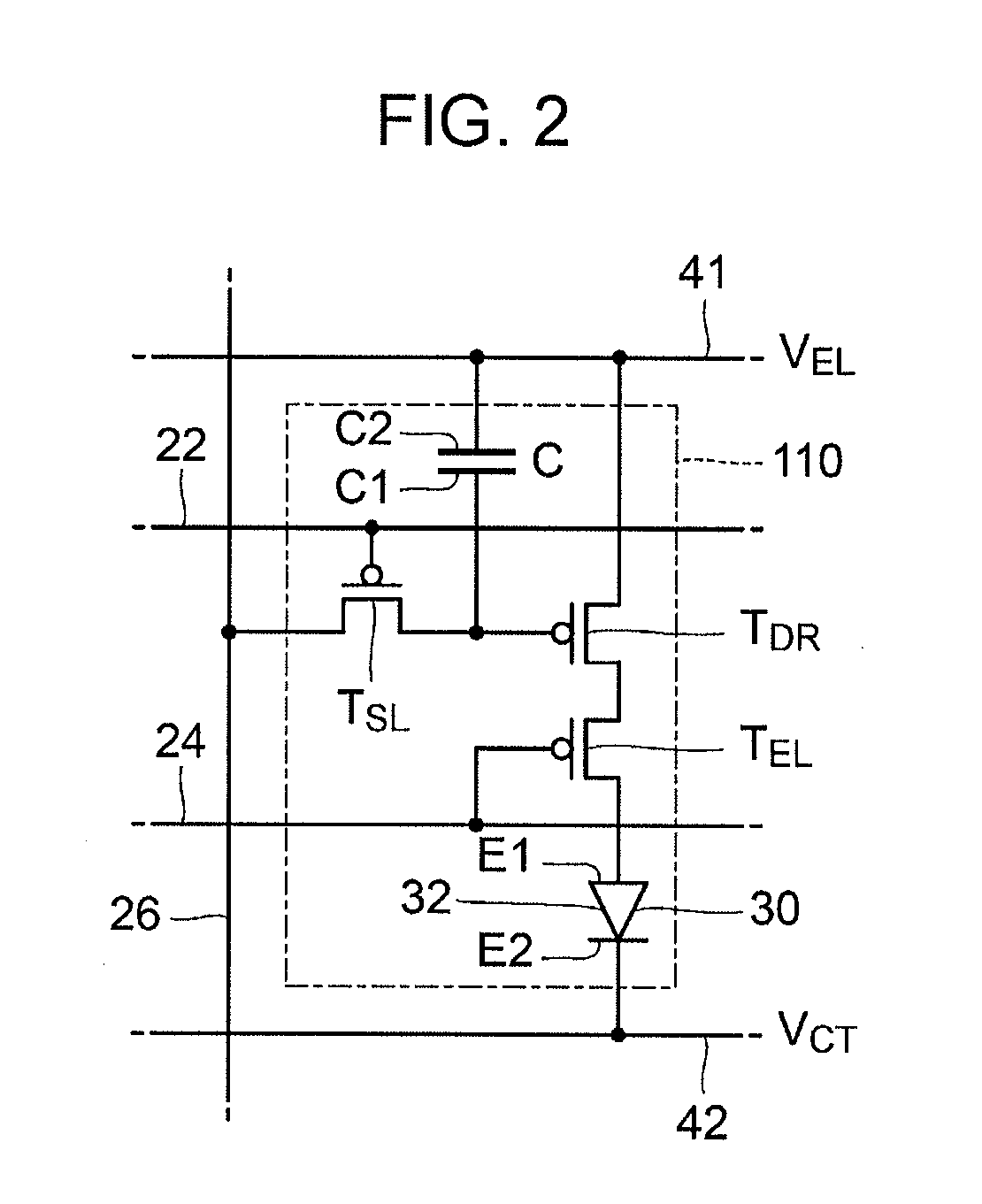
[0028]The element substrate 10 is provided with a display section 12 and a peripheral circuit section 14 (see FIG. 3). The display section 12 has a plurality of pixels 20 arranged therein. An organic EL element 30 is disposed as a light-emitting element for each pixel 20. Specifically, the element substrate 10 includes a pixel 20B in which blue (B) light is obtained, a pixel 20...

embodiment 2

Electronic Apparatus

[0090]Referring to FIG. 6, an electronic apparatus according to this embodiment is described. In this embodiment, an example of an electronic apparatus includes a head-mounted display, hereinafter referred to as HMD, equipped with an organic EL device. FIG. 6 is a schematic view illustrating the optical structure of a head-mounted display according to Embodiment 2 of the invention.

[0091]An HMD200 is, as illustrated in FIG. 6, a see-through type with which a user can visually recognize both the display of the HMD200 and an outside scene. The HMD200 includes a pair of optical units 214a and 214b to display information, a temple section mounted on the head (not shown), a power supply and a control section (not shown), etc. In the HMD200, the optical units 214a and 214b display various information visible to the user's eyes. The user can visually recognize such information and the outside scene (view) at the same time. Here, the optical units 214a and 214b are config...

modified example 1

[0102]In descriptions of the organic EL elements 30 in the above embodiments, white-light emission is assumed, but the color of light emitted is not limited to white. For example, an organic EL element may be configured to emit light with a desired color for each of the pixels 20B, 20G, and 20R. According to this configuration, in addition to the advantages in the above embodiments, the color filter layer 50 can be removed.


PUM


Abstract

An electro-optic device includes an element substrate. The element substrate has a display section and a peripheral circuit section. The display section has a plurality of pixels arranged therein. The peripheral circuit section is disposed around the display section and contains peripheral circuits. The display section has, for each pixel, an organic EL element and a transistor for driving the organic EL element. The organic EL element is disposed above the transistor with a light-reflective layer and an insulating layer in between. The insulating layer has a different film thickness in accordance with to the display color of the pixel. An insulating layer in the peripheral circuit section has the same layer structure as the insulating layer having a largest film thickness in the display section.

Description

BACKGROUND[0001]1. Technical Field[0002]The present invention relates to an electro-optic device and an electronic apparatus.[0003]2. Related Art[0004]A known electro-optic device includes a light-emitting device equipped with a light-emitting element for each of multiple pixels arranged in a display area. In such a light-emitting device, a wire to supply current to an electrode of the light-emitting element is connected so that the light-emitting element can emit light. For example, JP-A-2015-76300 proposes a light-emitting device in which a second electrode and peripheral wiring formed around the display area are connected to enable sufficient conduction between wires to supply current and the second electrode (cathode) of the light-emitting element.[0005]The light-emitting device in JP-A-2015-76300 is configured to appropriately adjust an optical path length between a first power electrical conductor and a second electrode of an optical resonator structure in accordance with the ...

Claims


Application Information

Patent Timeline
Patent Type & Authority Applications(United States)
IPC IPC(8): H01L27/32H01L51/52
CPCH01L27/3258H01L27/3276H01L27/3272H01L27/3246H01L27/3262H01L27/3211H01L27/322H01L51/5271G09G3/3208H10K59/30H10K59/00H10K59/35H10K59/38H10K59/124H10K59/131H10K50/852H10K50/856H10K50/865H10K2102/341H10K2102/3026H10K2102/351H10K59/122H10K59/126H10K59/1213
Inventor OTA, HITOSHI
Owner SEIKO EPSON CORP
Why Eureka
Try Eureka