
Display panel and repairing method thereof

a technology for repairing and display panels, applied in the direction of electrical devices, semiconductor devices, instruments, etc., can solve the problems of difficult rework of display panels, inability of pixel units to emit light, and dark spots that might appear

Inactive Publication Date: 2016-12-01
AU OPTRONICS CORP
View PDF2 Cites 47 Cited by
  • Summary
  • Abstract
  • Description
  • Claims
  • Application Information

AI Technical Summary

Benefits of technology

The present invention provides a display panel with a redundancy of bonding pads, which allows for the replacement of a defective light-emitting device on the same pixel unit with a substitutive light-emitting device. This ensures that each pixel unit includes at least one functioning light-emitting device that can emit light of the desired color. The technical effect of this invention is improved manufacturing efficiency and improved reliability of the display panel.

Problems solved by technology

When any one of the LEDs is damage or is loss during the manufacturing process, the pixel unit would not be able to emit light and therefore dark spots might be appeared on the LED display panel.
However, display panels are difficult to rework and the manufacturing process of the display panels is complicated.

Method used


Image

  • Display panel and repairing method thereof
  • Display panel and repairing method thereof
  • Display panel and repairing method thereof

Examples


Embodiment Construction

[0024]To provide a better understanding of the present disclosure, preferred embodiments will be made in detail. The preferred embodiments of the present disclosure are illustrated in the accompanying drawings with numbered elements.

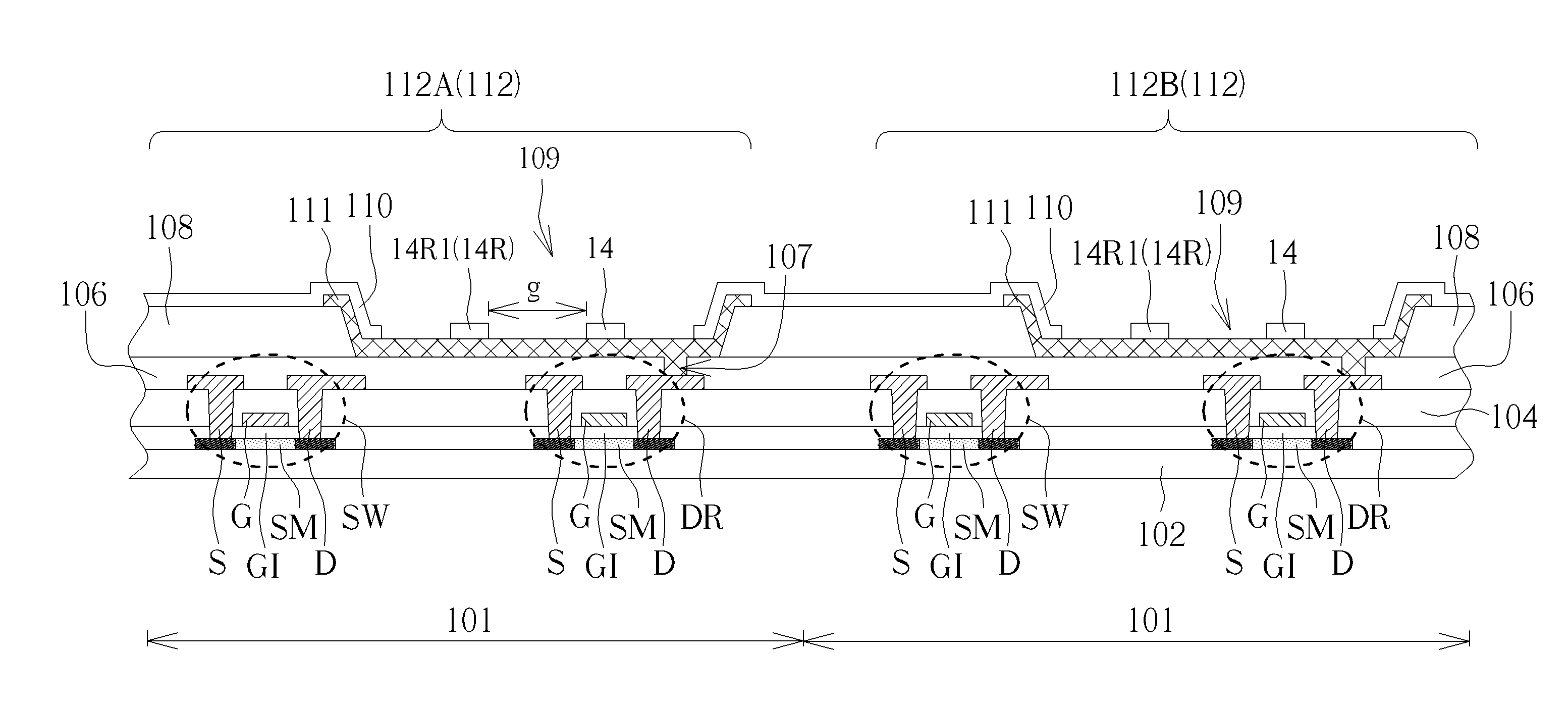
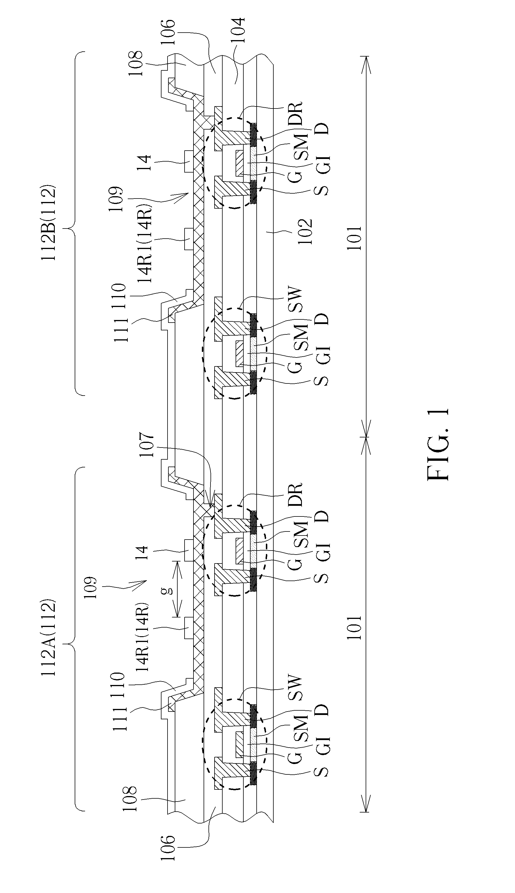
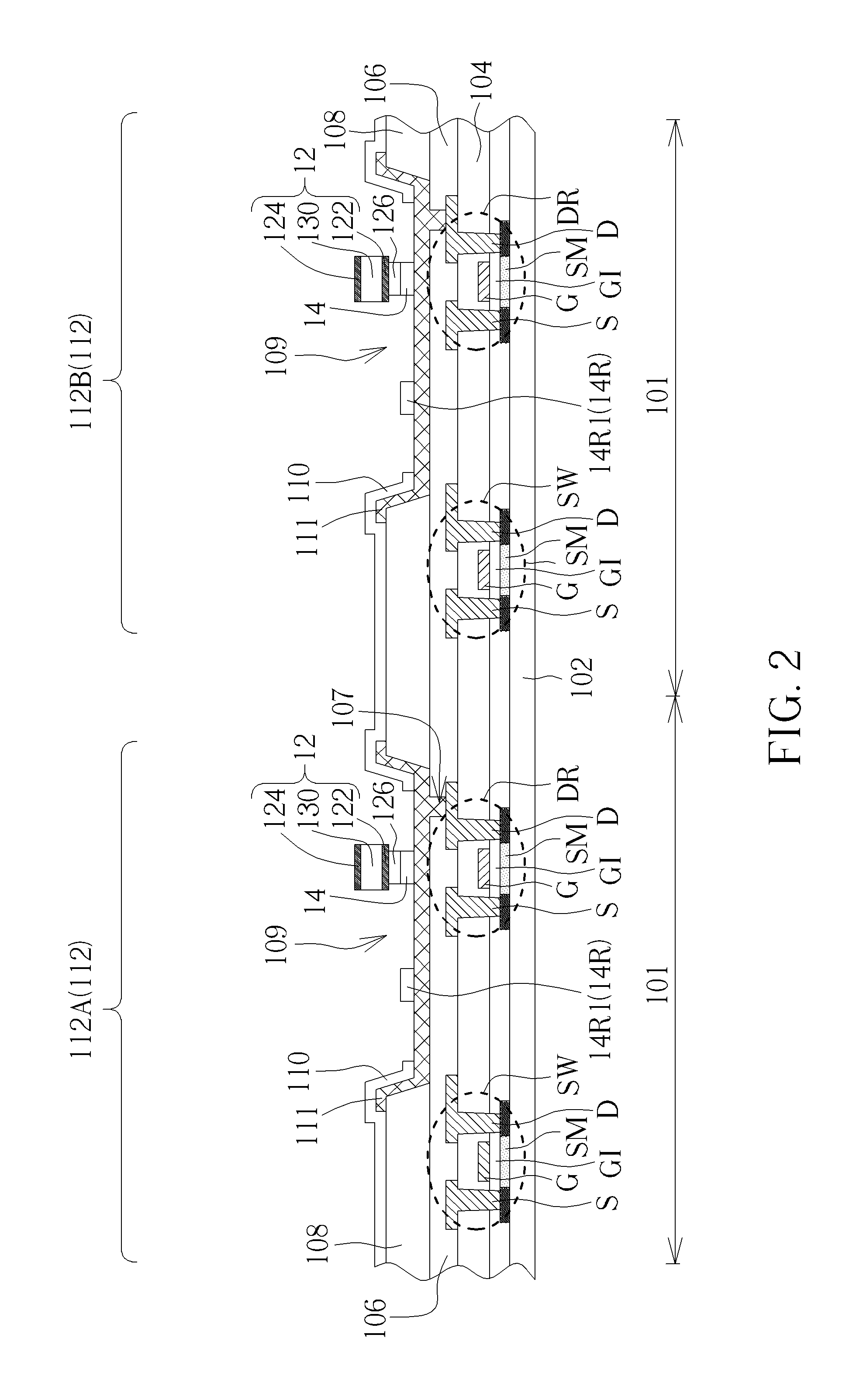
[0025]Refer to FIGS. 1-4. FIGS. 1-2 are schematic diagram illustrating a method of fabricating a display panel according to a first embodiment of the present disclosure, FIG. 3 is a top view diagram of the display panel according to the first embodiment the present disclosure, and FIG. 4 is an equivalent circuit diagram of the display panel according to the first embodiment of the present disclosure. As shown in FIG. 1, a substrate 102 having a plurality of pixel regions 101 is provided. The substrate 102 may comprise a rigid substrate or a flexible substrate e.g. a glass substrate or a plastic substrate, but not limited thereto. Then, a plurality of pixel units 112 are formed in the pixel regions 101 respectively on the substrate 102. The pixel units 11...


PUM


Abstract

A method for repairing a display panel includes the following steps. A display panel is provided. The display panel includes a substrate and a plurality of pixel units. The pixel units are disposed on the substrate, wherein each pixel unit includes at least one bonding pad, at least one light-emitting device and at least one first substitutive bonding pad. The bonding pad is disposed on the substrate. The light-emitting unit is disposed on the bonding pad and is electrically connected to the bonding pad. The first substitutive bonding pad is disposed on the substrate. A defect detecting process is performed to detect whether the light-emitting device of each pixel unit is defective or not. A repairing process is performed to form a first substitutive light-emitting device on the first substitutive bonding pad when a light-emitting device of a pixel unit is found defective.

Description

BACKGROUND OF THE DISCLOSURE[0001]1. Field of the Disclosure[0002]The present disclosure relates to a display panel and repairing method thereof, and more particularly, to a display panel and repairing method thereof with substitutive bonding pads.[0003]2. Background of the Disclosure[0004]With the progress of optoelectronics and related technologies, electronic products, such as personal digital assistant (PDA), mobile phone, smart phone and notebook (NB) are getting popular. As the demands for those electronic products are increased, the display screen / panel, which plays an important role in those electronic products, has become the primary objective to designers in this field.[0005]Due to its advantages such as environment friendly, high photoelectric conversion efficiency, compact size, long lifetime, controllable wavelength and low heat generation, light emitting diodes (LED) have been widely used in the display panel. For example, from the large display boards in the city to t...

Claims


Application Information

Patent Timeline
IPC IPC(8): G09G3/00G09G3/32
CPCG09G3/32G09G3/006G09G3/3233G09G2330/10H01L25/0753H10K71/861H10K59/12
Inventor CHEN, CHANG-CHANHSU, WEN-PINLIU, PIN-MIAO
Owner AU OPTRONICS CORP
Learn More