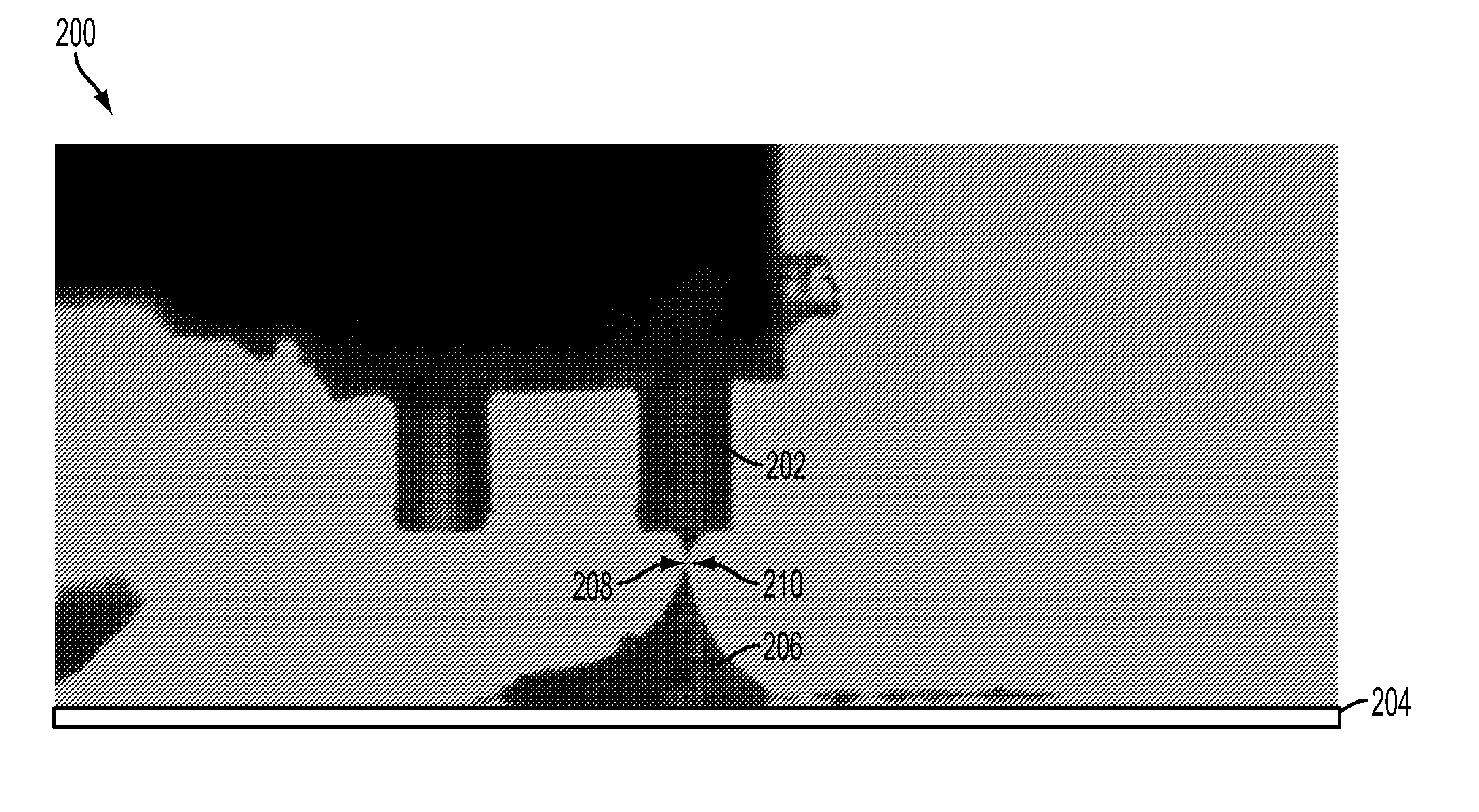
Self assembly of field emission tips by capillary bridge formations
a field emission tip and formation technology, applied in the field of manufacturing processes, can solve the problems of time-consuming and costly present manufacturing techniques, significant current emission at relatively low gate voltage,
- Summary
- Abstract
- Description
- Claims
- Application Information
AI Technical Summary
Benefits of technology
Problems solved by technology
Method used
Image
Examples
Embodiment Construction
[0016]Conductive sharp tips are of particular interest due to the high electric fields they generate when charged to a sufficient potential. The presence of high charge density and strong electric field help pull electrons off the tip easily leading to the creation of a field emission device. These field emission devices find applications in microscopy and field emission displays, among other areas. The following describes a method and system to create such sharp tips, which are identified by having surfaces with High Gaussian Curvatures.
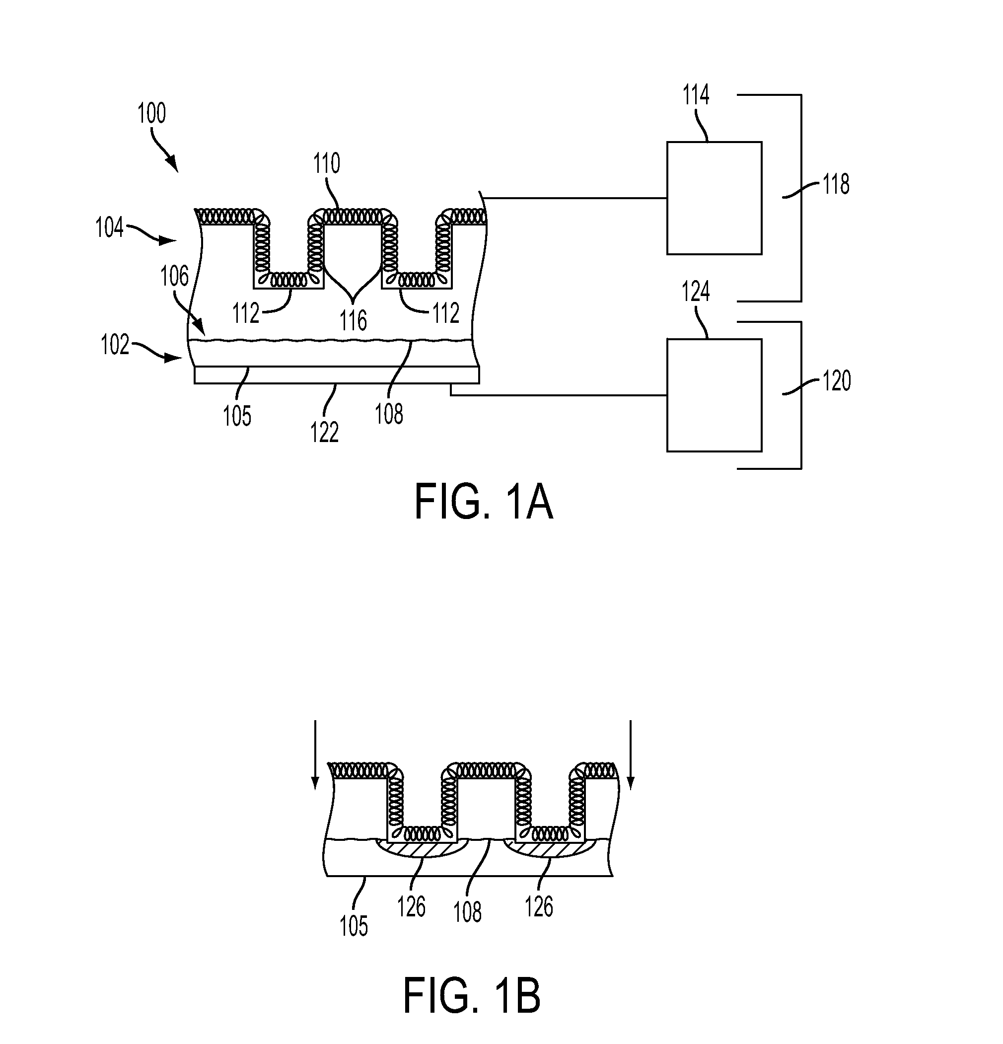
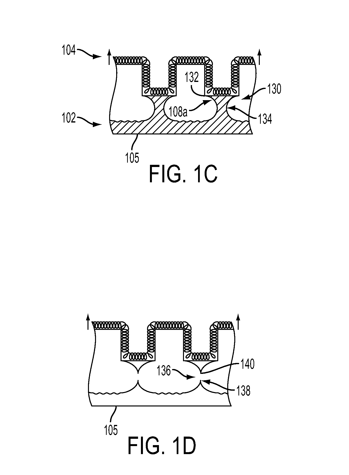
[0017]Turning to FIGS. 1A-1D, illustrated is a system configuration 100 designed to perform a series of process step to produce sharp conductive tips, via a capillary bridge type formation. More particularly, as shown in FIG. 1, system configuration 100 includes a first side 102 and a second side 104. The first side includes a first surface 106, on which is located a material 108. In some embodiments, first side 102 includes a substrate 105, wherein...
PUM
 Abstract
Description
Claims
Application Information
 - R&D
- Intellectual Property
- Life Sciences
- Materials
- Tech Scout
- Unparalleled Data Quality
- Higher Quality Content
- 60% Fewer Hallucinations
Browse by: Latest US Patents, China's latest patents, Technical Efficacy Thesaurus, Application Domain, Technology Topic, Popular Technical Reports.
© 2025 PatSnap. All rights reserved.Legal|Privacy policy|Modern Slavery Act Transparency Statement|Sitemap|About US| Contact US: help@patsnap.com


