
Self-aligned filter for an image sensor

Active Publication Date: 2009-08-13
OMNIVISION TECH INC
View PDF5 Cites 211 Cited by
  • Summary
  • Abstract
  • Description
  • Claims
  • Application Information

AI Technical Summary

Benefits of technology

[0017]For some embodiments, the filter may be a color filter, a black, a white filter, etc. The semiconductor substrate may be a silicon substrate. The insulator material may be silicon oxide. The passivation layer may be silicon nitride.
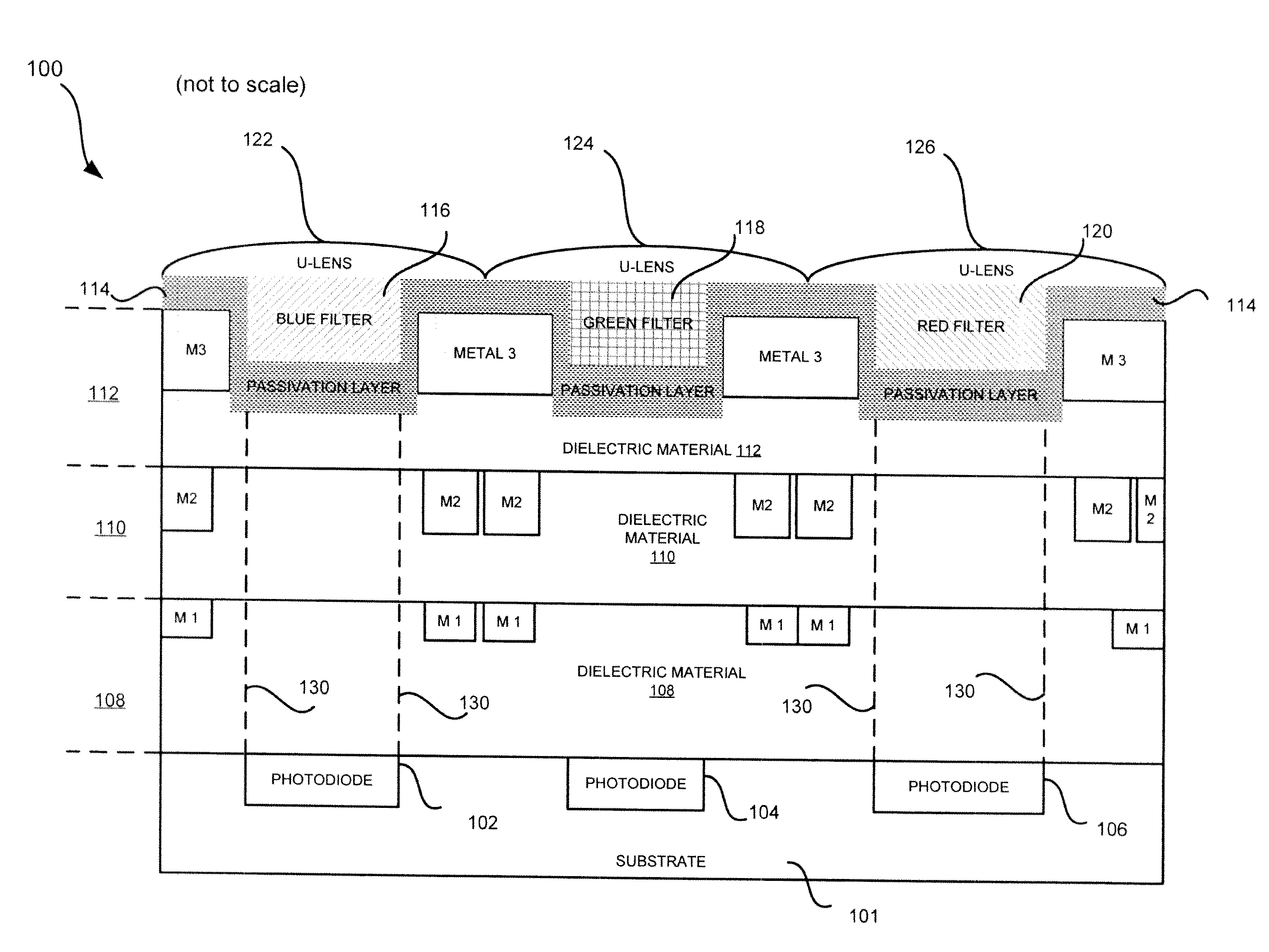
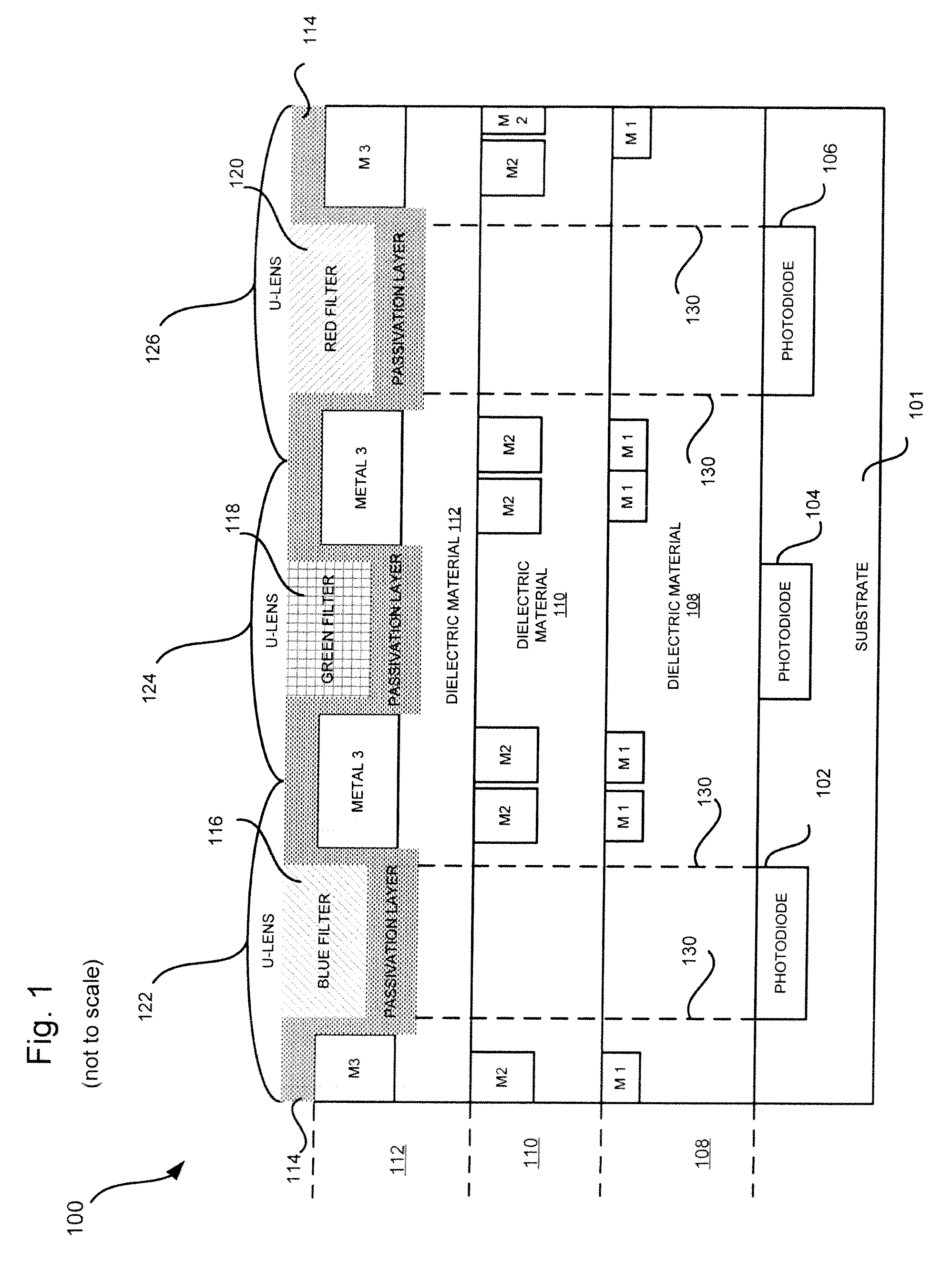
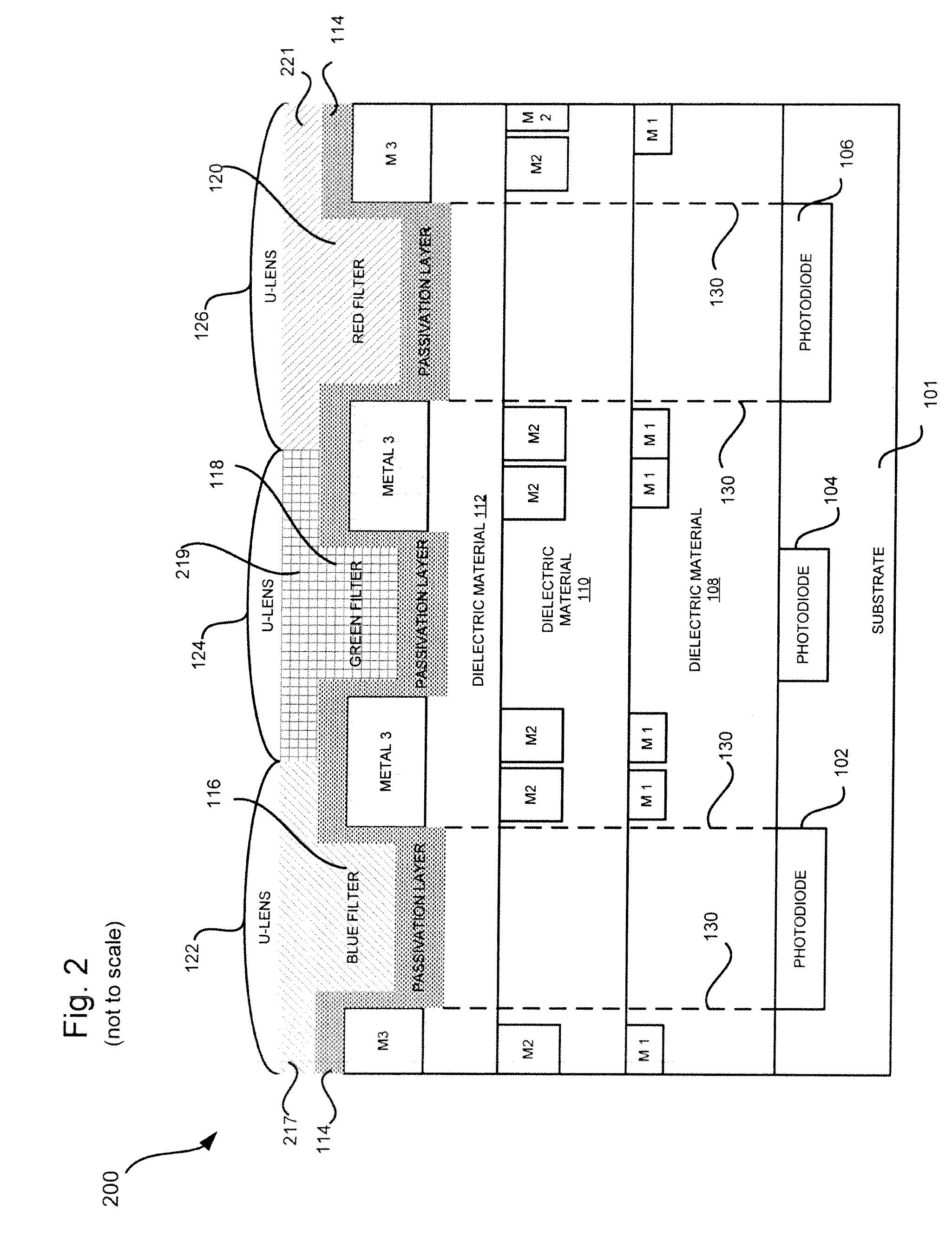
[0018]One advantage of embodiments of the present invention is that because the filters are self-aligned over the photosensitive element the crosstalk among pixels may be reduced. Another advantage of embodiments of the present invention is that because the filter is placed between the metal conductors rather than on the surface of the metal conductors or other layers making up the image sensor, a thicker filter may be used without increasing the overall height of the pixel stack. That is, the height of the layers of material making up the pixel can be increased without increasing the distance between the micro-lens and the substrate surface. Other features and advantages of the present invention will be apparent from the accompanying drawings and from the detailed description that follows.

Problems solved by technology

Conventional image sensors suffer from some limitations, however.
When the image sensor has a relatively low sensitivity the image sensor does not collect enough light.
The result is that the reproduced image can be too dark.
Low sensitivity is particularly troublesome as devices are scaled smaller and smaller.
One source of low sensitivity is in devices with smaller pixels; it can be difficult to get light into the smaller pixels.
Another limitation of image sensors concerns crosstalk.
The result is noise, which can cause a degraded reproduction of the image.

Method used


Image

  • Self-aligned filter for an image sensor
  • Self-aligned filter for an image sensor
  • Self-aligned filter for an image sensor

Examples


Embodiment Construction

[0013]In the below description, numerous specific details, such as, for example, particular processes, materials, devices, and so forth, are presented to provide a thorough understanding of embodiments of the invention. One skilled in the relevant art will recognize, however, that the embodiments of the present invention may be practiced without one or more of the specific details, or with other methods, components, etc. In other instances, structures or operations are not shown or described in detail to avoid obscuring the understanding of this description.

[0014]Reference throughout this specification to “one embodiment” or “embodiment” means that a particular feature, structure, process, block, or characteristic described in connection with an embodiment is included in at least one embodiment of the present invention. Thus, the appearance of the phrases “in one embodiment” or “in an embodiment” in various places throughout this specification does not necessarily mean that the phra...


PUM


Abstract

An image sensor includes at least one photosensitive element disposed in a semiconductor substrate. Metal conductors may be disposed on the semiconductor substrate. A filter may be disposed between at least two individual metal conductors and a micro-lens may be disposed on the filter. There may be insulator material disposed between the metal conductors and the semiconductor substrate and / or between individual metal conductors. The insulator material may be removed so that the filter may be disposed on the semiconductor substrate.

Description

BACKGROUND[0001]1. Field[0002]Embodiments of the present invention relate to image sensors and, in particular, to color filters for image sensors.[0003]2. Discussion of Related Art[0004]In general, conventional image sensors perform well to generate images. A typical image sensor may be fabricated using a complementary metal oxide semiconductor (CMOS) technology. Charge coupled device (CCD) technology is also suitable.[0005]Conventional image sensors suffer from some limitations, however. When the image sensor has a relatively low sensitivity the image sensor does not collect enough light. The result is that the reproduced image can be too dark. Low sensitivity is particularly troublesome as devices are scaled smaller and smaller. One source of low sensitivity is in devices with smaller pixels; it can be difficult to get light into the smaller pixels.[0006]Another limitation of image sensors concerns crosstalk. Crosstalk occurs when light designated for one pixel enters an adjacent ...

Claims


Application Information

Patent Timeline
IPC IPC(8): H01L31/00G01T1/24
CPCH01L27/14621H01L27/14625H01L27/14627H01L27/14687H01L27/14645H01L27/14685H01L27/14632
Inventor TAI, HSIN-CHIHMAO, DULIVENEZIA, VINCENTQIAN, WEIDONGSHAH, ASHISHRHODES, HOWARD E.
Owner OMNIVISION TECH INC
Learn More