
Semiconductor package and the method of making the same

Active Publication Date: 2008-09-25
ADVANCED SEMICON ENG INC
View PDF99 Cites 277 Cited by
  • Summary
  • Abstract
  • Description
  • Claims
  • Application Information

AI Technical Summary

Benefits of technology

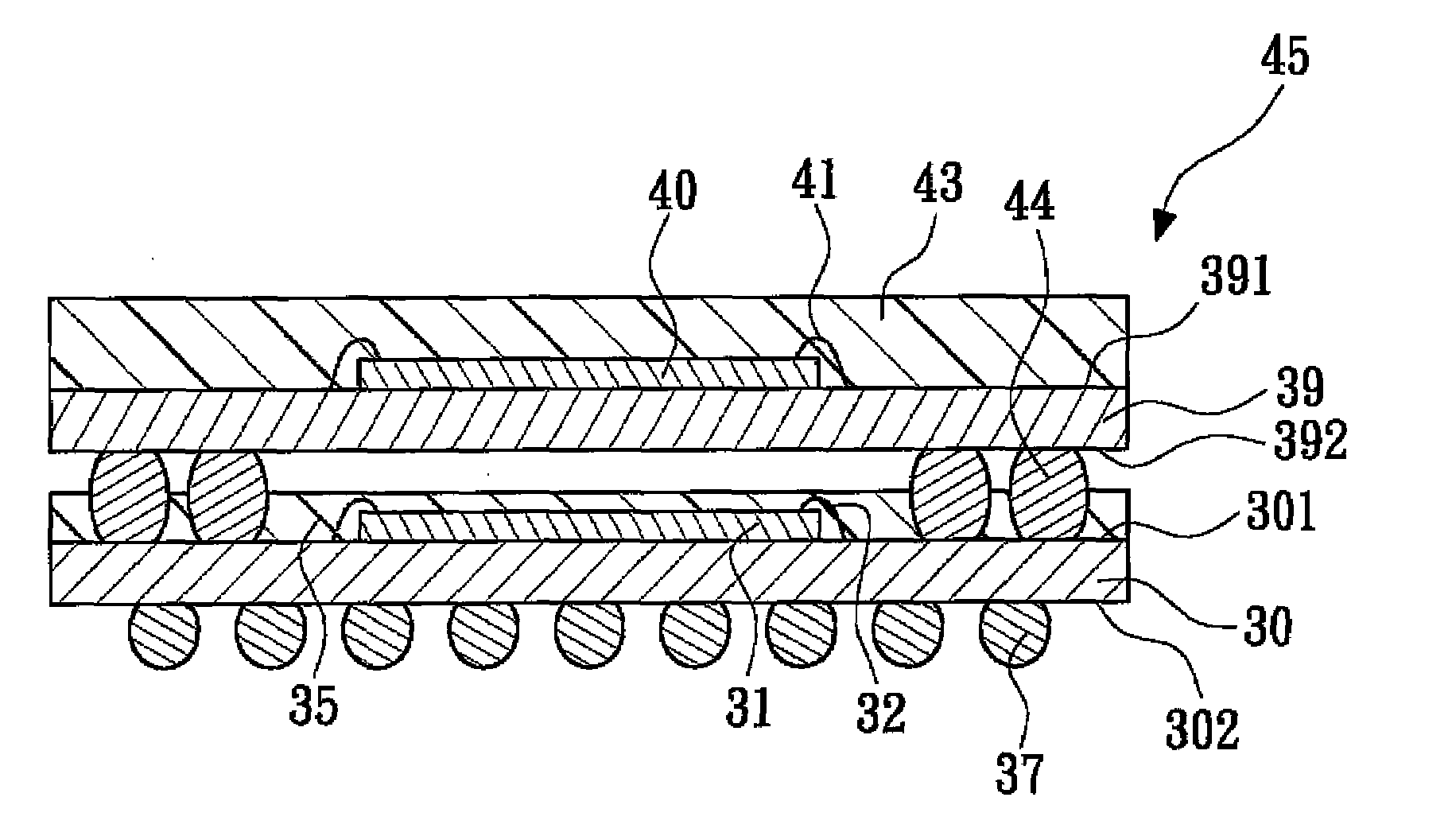
[0014]The present invention is further directed to a semiconductor package, which comprises a first substrate, a first chip, a second substrate, a second chip, a plurality of fourth solder balls and a first molding compound. The first substrate has a first surface and a second surface. The first chip is mounted onto the first surface of the first substrate, and is electrically connected to the first substrate. The second substrate has a first surface and a second surface. The second chip is mounted onto the first surface of the second substrate, and is electrically connected to the second substrate. The fourth solder balls connect the second surface of the second substrate and the first surface of the first substrate. The first molding compound encapsulates the first surface of the first substrate, the chip and parts of the fourth solder balls, and the height of the first molding compound is smaller than the height of each of the fourth solder balls. Thus, in the present invention, the first molding compound encapsulates the entire first surface of the first substrate, so that the mold flush of the first molding compound will not occur, and the rigidity of the first substrate is increased.

Problems solved by technology

Therefore, the area for mounting the first solder balls 15 is polluted, causing the failure of the ball-mounting process and defects in the package.

Method used


Image

  • Semiconductor package and the method of making the same
  • Semiconductor package and the method of making the same
  • Semiconductor package and the method of making the same

Examples


first embodiment

[0018]FIGS. 8 to 13 are schematic views of each step of the method of making a semiconductor package according to the present invention. In FIG. 8, a first substrate 30 having a first surface 301 and a second surface 302 is provided. Afterward, a first chip 31 is mounted onto the first surface 301 of the first substrate 30, and is electrically connected to the first substrate 30. In the embodiment, the first chip 31 is electrically connected to the first substrate 30 via a plurality of first wires 32. Afterward, a plurality of conductive elements 33 is formed on the first surface 301 of the first substrate 30. In the embodiment, the conductive elements 33 are a plurality of first solder balls, which are spherical.

[0019]In FIG. 9, a mold 34 is used to cover the conductive elements 33. The mold 34 has a plurality of cavities 341. Each of the cavities 341 accommodates top ends of each of the conductive elements 33, and top ends of the conductive elements 33 contact with the cavities 34...

second embodiment

[0031]FIGS. 14 to 19 are schematic views of each step of the method of making a semiconductor package according to the present invention. In FIG. 14, a first substrate 50 is provided. The first substrate 50 has a first surface 501 and a second surface 502. A first chip 51 is mounted onto the first surface 501 of the first substrate 50, and is electrically connected to the first substrate 50. In the embodiment, the first chip 51 is electrically connected to the first substrate 50 via a plurality of first wires 52. Afterward, a plurality of conductive elements 53 is formed on the first surface 501 of the first substrate 50. In the embodiment, the conductive elements 53 are a plurality of first solder balls, which are spherical.

[0032]In FIG. 15, a mold 54 is used to cover the conductive elements 53. The mold 54 has a plurality of protrusions 541, and each of the protrusions 541 contacts top ends of each of the conductive elements 53.

[0033]In FIG. 16, a molding process is performed to e...


PUM


Abstract

The present invention relates to semiconductor package and the method of making the same. The method of the invention comprises the following steps: (a) providing a first substrate; (b) mounting a first chip onto a surface of the first substrate; (c) forming a plurality of conductive elements on the surface of the first substrate; (d) covering the conductive elements with a mold, the mold having a plurality of cavities accommodating top ends of each of the conductive elements; and (e) forming a first molding compound for encapsulating the surface of the first substrate, the first chip and parts of the conductive elements, wherein the height of the first molding compound is smaller than the height of each of the conductive elements. Thus, the first molding compound encapsulates the entire surface of the first substrate, so that the mold flush of the first molding compound will not occur, and the rigidity of the first substrate is increased.

Description

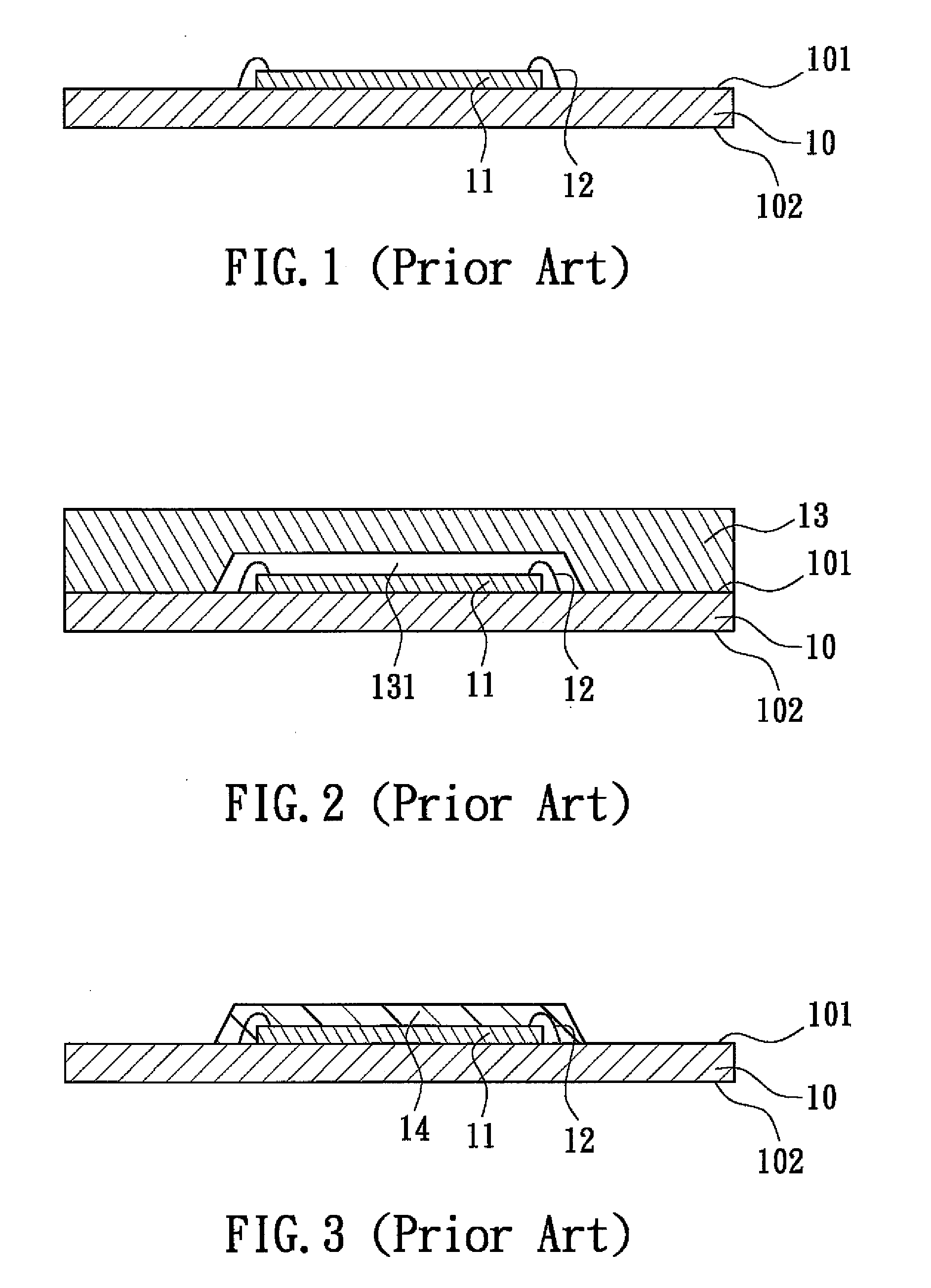
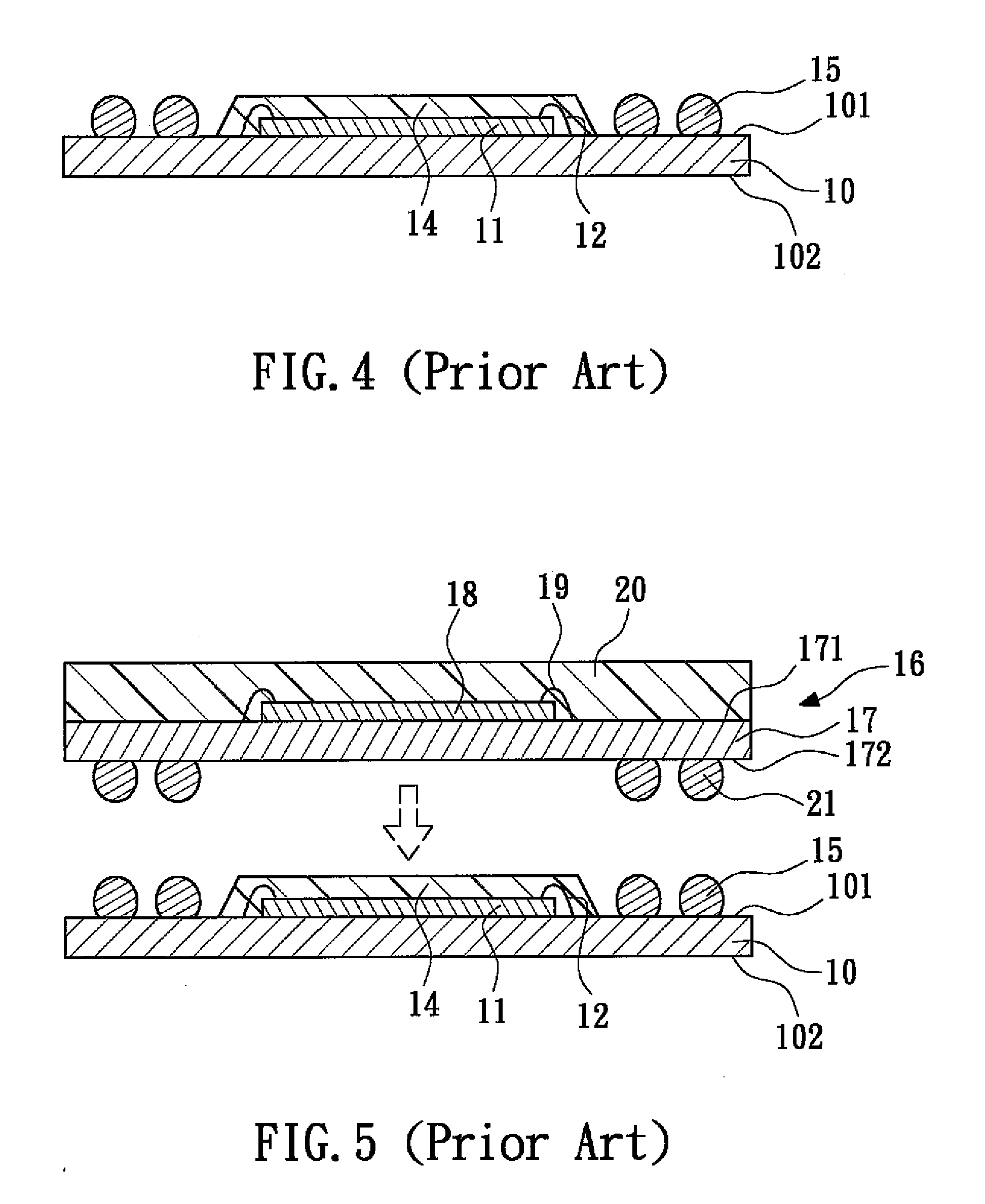
BACKGROUND OF THE INVENTION[0001]1. Field of the Invention[0002]The present invention relates to a semiconductor package and the method of making the same, and more particularly to a stacked semiconductor package and the method of making the same.[0003]2. Description of the Related Art[0004]FIGS. 1 to 7 are schematic views of each step of the method of making a conventional stacked semiconductor package. First, referring to FIG. 1, a first substrate 10 is provided. The first substrate 10 has a first surface 101 and a second surface 102. Afterward, a first chip 11 is mounted onto the first surface 101 of the first substrate 10, and is electrically connected to the first substrate 10 via a plurality of first wires 12.[0005]In FIG. 2, a mold 13 is used to cover the first surface 101 of the first substrate 10. The mold 13 has a cavity 131 for accommodating the first chip 11 and the first wires 12.[0006]As shown in FIG. 3, a molding process is performed to encapsulate the first chip 11 a...

Claims


Application Information

Patent Timeline
IPC IPC(8): H01L23/12H01L21/50
CPCH01L21/565H01L23/3128H01L2924/15321H01L2224/73265H01L2224/48227H01L2224/32225H01L2225/1058H01L2225/1023H01L2924/3511H01L24/48H01L25/105H01L2924/15311H01L2924/15331H01L2924/00012H01L2924/00H01L24/73H01L2924/181H01L2924/00014H01L2224/45099H01L2224/45015H01L2924/207
Inventor SUN, YU-CHINGCHENG, REN-YIWAN, TSAIHSU, CHIH-HUNGCHEN, KUANG-HSIUNG
Owner ADVANCED SEMICON ENG INC
Learn More