Specialized processing block for programmable logic device
a technology of programmable logic and processing blocks, applied in the field of special processing blocks, can solve the problems of increasing complexity of applications for which plds are used, limited rounding limited saturation capabilities of known dsp blocks, so as to achieve the effect of improving rounding and saturation capabilities
- Summary
- Abstract
- Description
- Claims
- Application Information
AI Technical Summary
Benefits of technology
Problems solved by technology
Method used
Image
Examples
embodiment 10
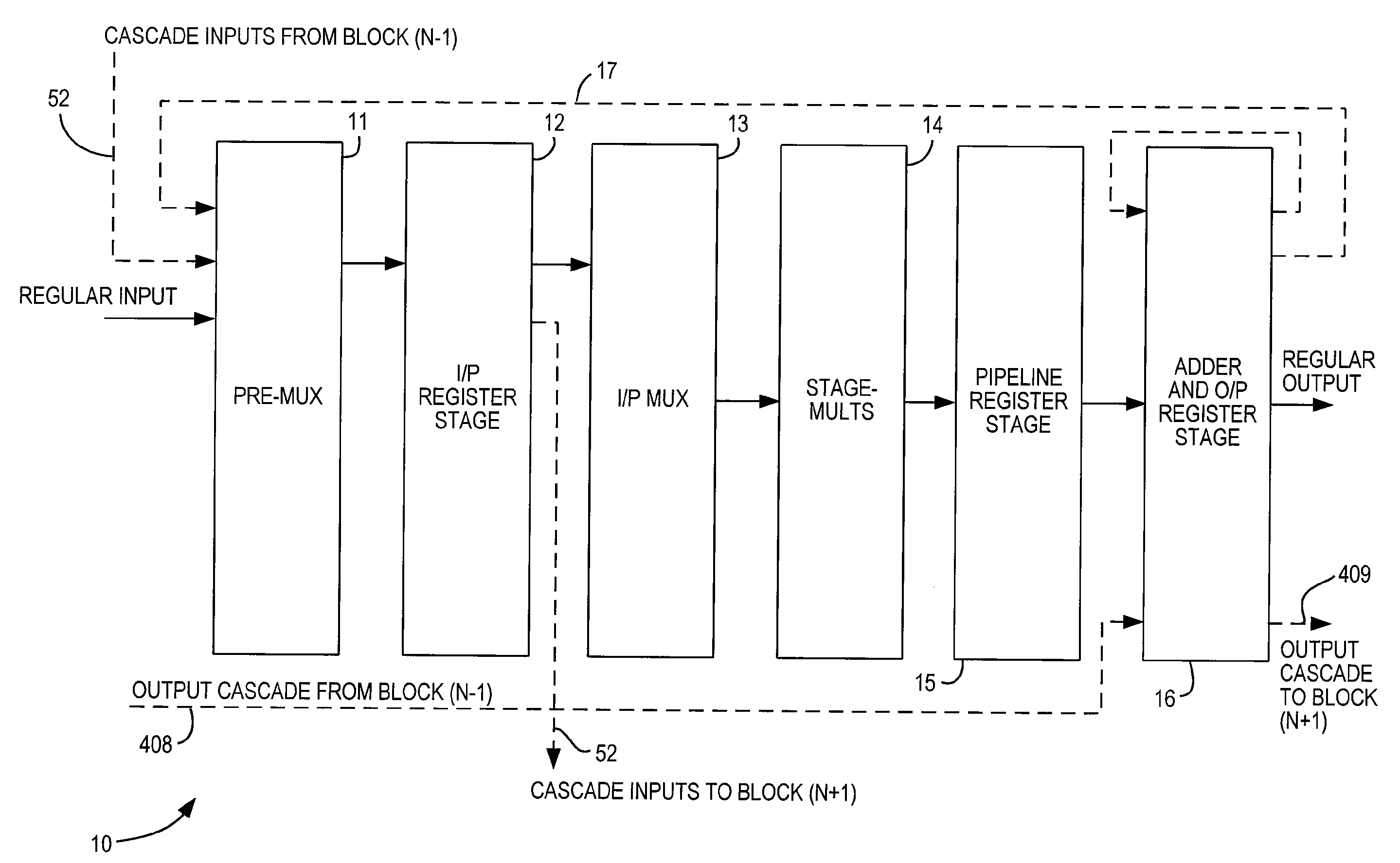
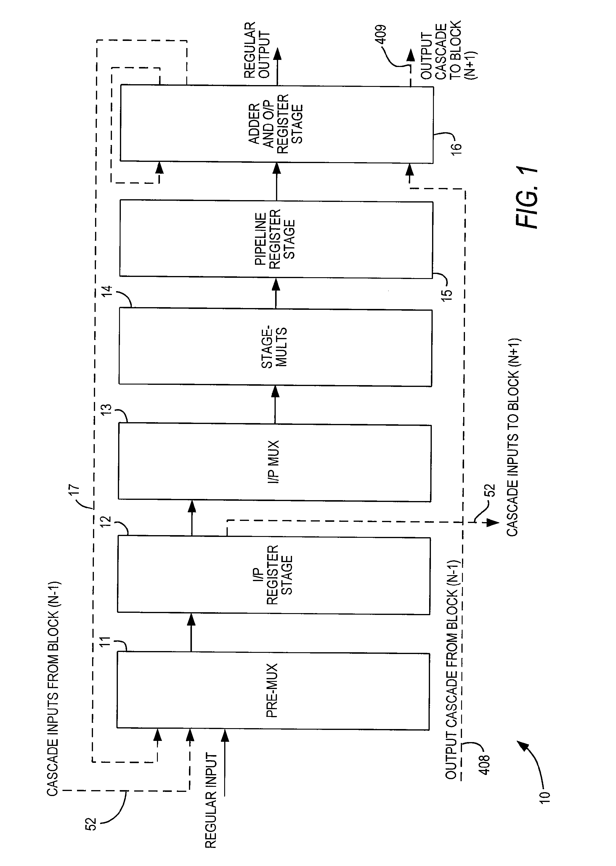
[0039]FIG. 1 shows a high-level diagram of one preferred embodiment 10 of a specialized processing block according to the invention, while FIG. 2 is a functional diagram of the same embodiment 10.
[0040]As seen in FIG. 1, specialized processing block 10 includes optional input pre-MUX stage 11, optional input register stage 12, optional input multiplexing stage 13, multiplication stage 14, optional pipeline register stage 15 and adder / output stage 16.
[0041]The function of input pre-MUX stage 11, if provided, is to format the regular inputs, loopback inputs and cascade inputs (see below) into a form suitable for registering.
[0042]Regular inputs do not require any specific formatting. Cascade inputs may be a one-register delayed version of a previous input, and therefore may need formatting accordingly. However, such formatting also can be done in programmable logic of the programmable logic device of which specialized processing block 10 is a part, so if formatting of cascade inputs i...
embodiment 70
[0076]The result, RNDSEL, is used, after the ORing of all RNDSEL bits as described above, as the control bit to select between rounded and unrounded values as shown, e.g., in FIGS. 7 and 8. In the embodiment 70 of FIG. 7, which may be programmably implemented in specialized processing block 10, the output of adder 71 is input to both rounding logic 60 and further adder 72. The output of rounding logic 60 is also input to adder 72, and controls whether or not adder 72 adds 1 to the output of adder 71. Because these rounding operations, as well as saturation operations in saturation logic 73, are in a critical path between registers 74, 75, the rounding and saturation operations must be completed within one clock cycle. This limits the maximum clock speed to one in which the rounding and saturation operations can be completed.
embodiment 80
[0077]Therefore, in embodiment 80 of FIG. 8, which may be programmably implemented in specialized processing block 10, instead of waiting for rounding logic 60 before performing addition 82, addition 71 and addition 82 are carried out simultaneously and the result of rounding logic 60 is used to control multiplexer 81, which selects between adders 71, 81. This look-ahead rounding decreases the time needed to perform rounding operations, and therefore increases the maximum permissible clock speed.
[0078]Similar clocking issues come into play when specialized processing block 10 is used in output cascade mode with another specialized processing block 10. As seen in embodiment 90 of FIG. 9, which may be programmably implemented in specialized processing block 10, the rounding and saturation circuitry 91 is located between cascade adder 92 and register 93. Once again, that places it in the critical path for register timing. Therefore, in the embodiment 100 shown in FIG. 10, which may be ...
PUM
 Abstract
Description
Claims
Application Information
 - R&D
- Intellectual Property
- Life Sciences
- Materials
- Tech Scout
- Unparalleled Data Quality
- Higher Quality Content
- 60% Fewer Hallucinations
Browse by: Latest US Patents, China's latest patents, Technical Efficacy Thesaurus, Application Domain, Technology Topic, Popular Technical Reports.
© 2025 PatSnap. All rights reserved.Legal|Privacy policy|Modern Slavery Act Transparency Statement|Sitemap|About US| Contact US: help@patsnap.com


