Bus arbitration method and semiconductor apparatus
a technology of bus and semiconductor, applied in the field of bus arbitration method, can solve the problems of inability to immediately respond to the method, difficult to detect the generation of a large number of bus requests, etc., and achieve the effect of improving the usability of the bus
- Summary
- Abstract
- Description
- Claims
- Application Information
AI Technical Summary
Benefits of technology
Problems solved by technology
Method used
Image
Examples
embodiment 1
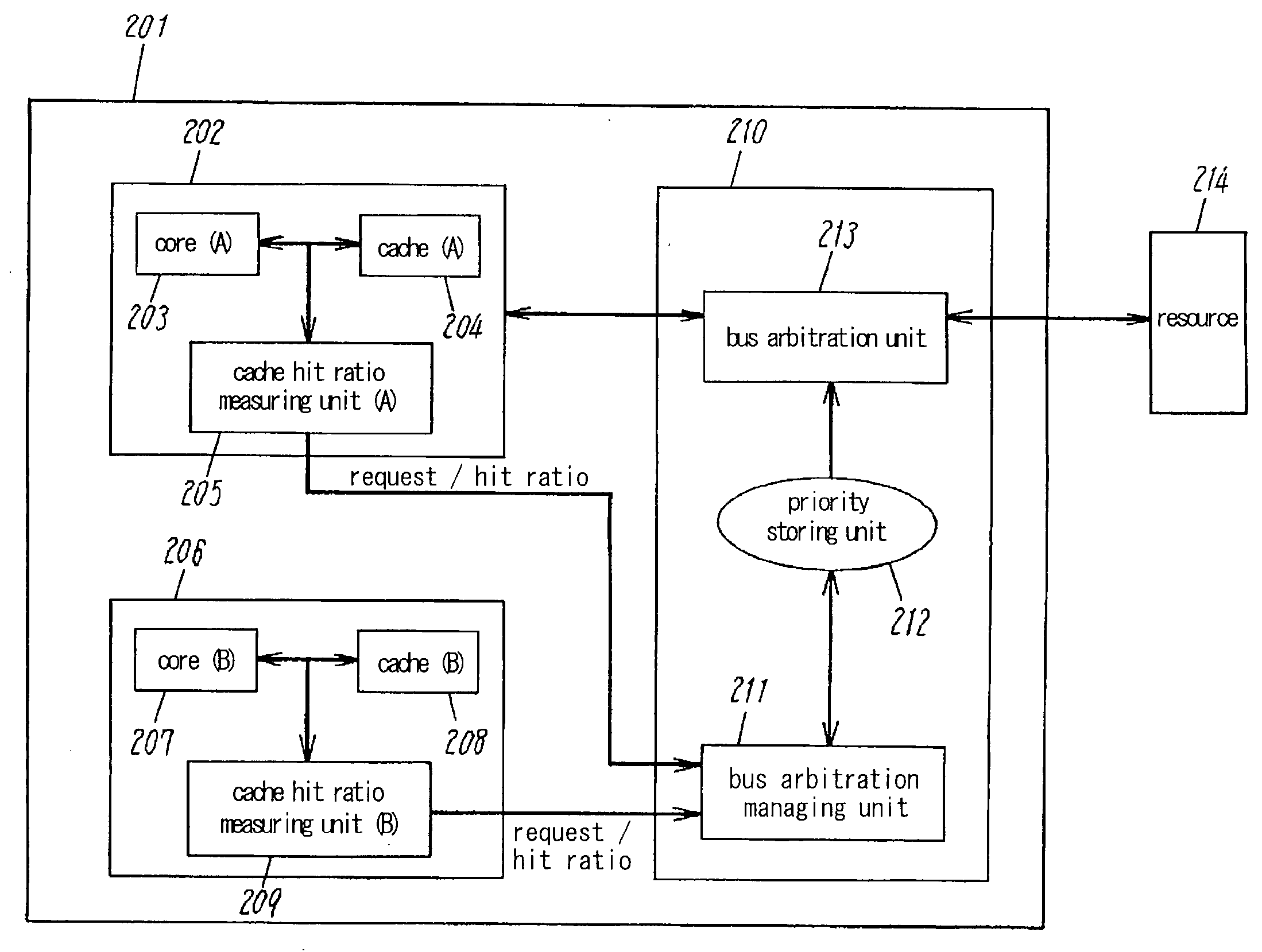
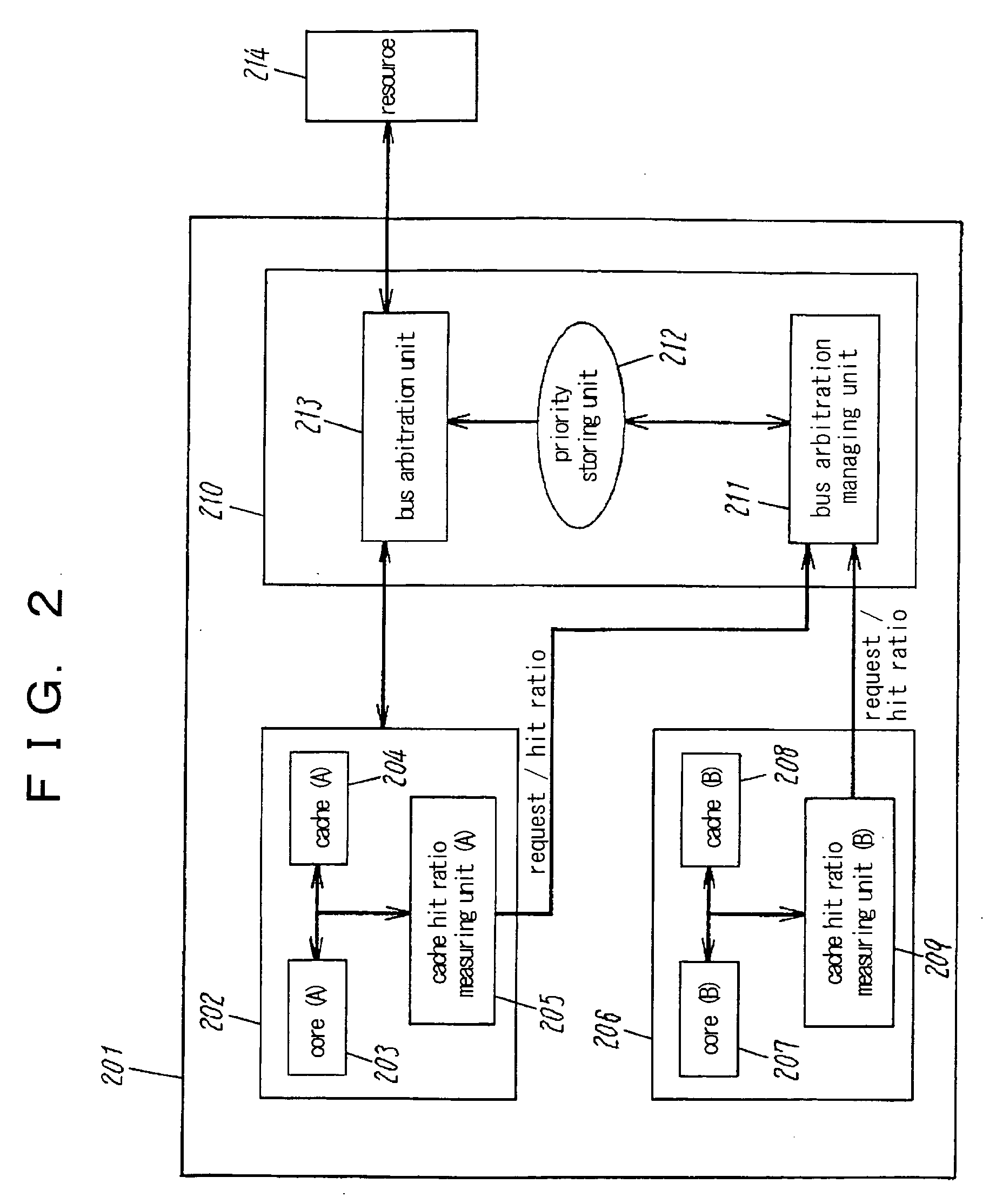
[0047]FIG. 2 shows an entire structure of a semiconductor apparatus according to an embodiment 1 of the present invention. FIG. 3 shows constitutions of cache hit ratio measuring units (A)205 and (B)209 and a bus arbitration managing unit 211 according to the embodiment 1. In the embodiment 1, the cache hit ratio measuring units (A)205 and (B)209 basically have a same structure, and these components (A)205 and (B)209 are referred to as a cache hit ratio measuring device 304 in the description below and FIG. 3.
[0048] The cache hit ratio measuring device 304 comprises a hit history register 301, a judging unit 302 and a request table 303. The bus arbitration managing unit 211 comprises a controller 306.
[0049] Next is described an operation of the semiconductor apparatus according to the embodiment 1. First, the cache accesses are recorded in the hit history register 301 by means of the FIFO method. The accesses are recorded a plurality of times wherein a hit is expressed as “1” and ...
embodiment 2
[0057]FIG. 2 shows an entire structure of a semiconductor apparatus according to an embodiment 2 of the present invention. A cache hit ratio measuring unit (A)205, a cache hit ratio measuring unit (B)209 and a bus arbitration managing unit 211 according to the embodiment 2 are shown in FIG. 5. The cache hit ratio measuring units (A)205 and (B)209 according to the embodiment 2 basically have a same constitution, and these components are referred to as a cache hit ratio measuring device 504 in the description below and FIG. 5.
[0058] As shown in FIG. 5, the cache hit ratio measuring device 504 comprises a hit history register 301, a judging unit 502, and a hit ratio code table 503.
[0059] Further, as shown in FIG. 6, the bus arbitration managing unit comprises a controller601 and a priority conversion table 602.
[0060] Next, operations of the foregoing components are described. The cache accesses are stored in the hit history register 301 by means of the FIFO method, wherein the hit i...
embodiment 3
[0067]FIG. 2 shows an entire structure of a semiconductor apparatus according to an embodiment 3 of the present invention. A cache hit ratio measuring unit (A)205 and a cache hit ratio measuring unit (B)209 according to the embodiment 3 are basically constituted in the same manner, and referred to as a cache hit ratio measuring device 706 in the description below and FIG. 7.
[0068] The ache hit ratio measuring device 706 comprises a plurality of hit history registers 701, 702 and 703, a judging unit 704 and a hit ratio conversion table 705. The cache hit ratio measuring device 706 operates in the same manner as described in the embodiment 2. More specifically, the cache hit ratio measuring device 706 measures the cache hit ratio to thereby read the hit ratio code corresponding to the measured cache hit ratio from a hit ratio code table 705 and output the read hit ratio code to the bus arbitration unit 211.
[0069] In the embodiment 3, the plurality of hit history registers 701, 702 a...
PUM
 Abstract
Description
Claims
Application Information
 - R&D
- Intellectual Property
- Life Sciences
- Materials
- Tech Scout
- Unparalleled Data Quality
- Higher Quality Content
- 60% Fewer Hallucinations
Browse by: Latest US Patents, China's latest patents, Technical Efficacy Thesaurus, Application Domain, Technology Topic, Popular Technical Reports.
© 2025 PatSnap. All rights reserved.Legal|Privacy policy|Modern Slavery Act Transparency Statement|Sitemap|About US| Contact US: help@patsnap.com


