
Display panel and array substrate thereof

a technology of array substrates and display panels, applied in static indicating devices, instruments, non-linear optics, etc., can solve problems such as easy crosstalk, and achieve the effect of improving user experiences

Active Publication Date: 2022-05-24
TCL CHINA STAR OPTOELECTRONICS TECH CO LTD
View PDF17 Cites 0 Cited by
  • Summary
  • Abstract
  • Description
  • Claims
  • Application Information

AI Technical Summary

Benefits of technology

This patent describes an array substrate for a display screen that reduces crosstalk and improves user experience by arranging pixel units with opposing polarities in rows and columns. The array substrate also includes data lines and dual scan lines to further reduce crosstalk and prevent the "head shaking stripy" phenomenon when human eyes view the screen.

Problems solved by technology

However, voltages of adjacent pixels along a vertical direction have same polarity and thus crosstalk is easy to be caused in the vertical direction.

Method used


Image

  • Display panel and array substrate thereof
  • Display panel and array substrate thereof
  • Display panel and array substrate thereof

Examples


Embodiment Construction

[0042]To make the objectives, technical schemes, and beneficial effects of the present application more clear and specific, the present application is described in further detail below with reference to the embodiments in accompanying with the appending drawings. It should be understood that the specific embodiments described herein are merely for explaining the present invention and the present invention is not limited thereto.

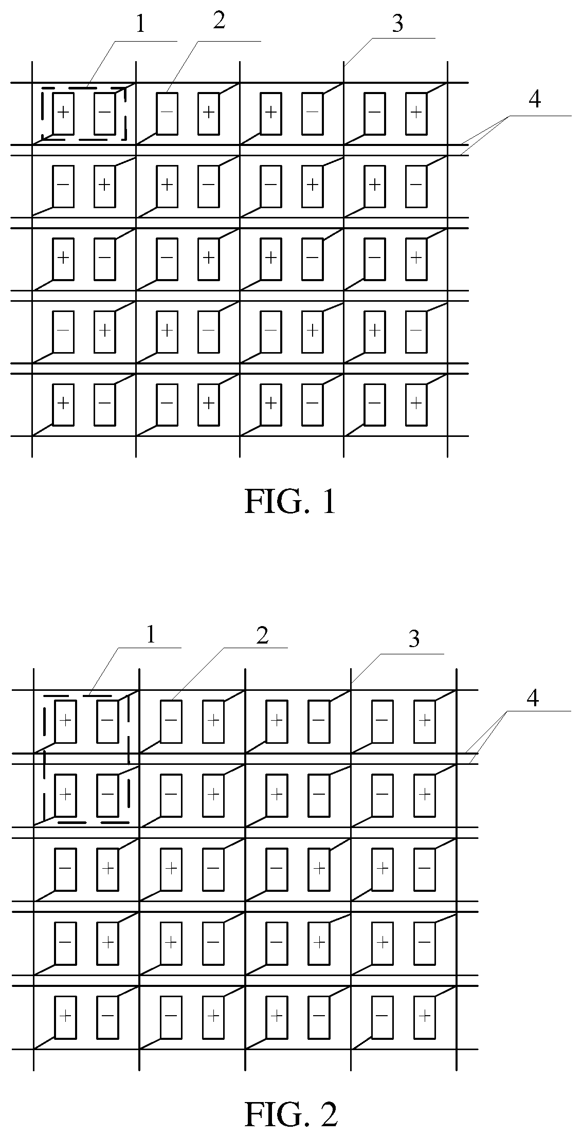
[0043]FIG. 1 is a schematic structural diagram illustrating an array substrate provided in accordance with an embodiment of the present application. The array substrate includes a plurality of pixel grouping units 1. Each of the pixel grouping units 1 includes at least two subpixels 2. The plurality of pixel grouping units 1 are arranged in rows and columns Adjacent pixel grouping units 1 arranged in a row direction have opposite polarities and adjacent pixel grouping units 1 arranged in a column direction have opposite polarities. The array substrate further...


PUM

PropertyMeasurementUnit
polaritiesaaaaaaaaaa
polarityaaaaaaaaaa
DC voltagesaaaaaaaaaa

Abstract

An array substrate and a display panel are provided, including a plurality of pixel grouping units, a plurality of data lines and a plurality of dual scan lines. Each of the pixel grouping units includes at least two subpixels. The plurality of pixel grouping units are arranged in rows and columns Adjacent pixel grouping units arranged in a row direction have opposite polarities and adjacent pixel grouping units arranged in a column direction have opposite polarities. Each of the data lines is located between any two adjacent columns of the pixel grouping units. Each of the plurality of dual scan lines is located between any two adjacent rows of the subpixels.

Description

FIELD OF THE DISCLOSURE[0001]The present application relates to liquid crystal panel industries, and more particularly to a display panel and an array substrate thereof.DESCRIPTION OF RELATED ARTS[0002]For liquid crystal display panels, liquid crystal molecules will be polarized after DC voltages are applied to the liquid crystal for a long time. To avoid the liquid crystal molecules being polarized, it needs to change the polarities of pixel electrode voltages periodically.[0003]Since column inversion is directed to the smallest source driving power, it is used to change the polarities of pixel electrode voltages for separated column such that same polarity is provided for a same column and different polarities are provided for adjacent columns When the liquid crystal panels are driven using the column inversion, voltages of adjacent data lines have opposite polarities. After brightness deviation is averaged spatially, a “flicker” phenomenon is diminished as compared to frame inver...

Claims


Application Information

Patent Timeline
Patent Type & Authority Patents(United States)
IPC IPC(8): G02F1/136G02F1/1362G09G3/36
CPCG02F1/136286G09G3/3614G02F1/1362G02F1/133G02F1/136222
Inventor YANG, HUI
Owner TCL CHINA STAR OPTOELECTRONICS TECH CO LTD
Learn More