Print element substrate, method of manufacturing print element substrate, and method of manufacturing printhead
a printing element and substrate technology, applied in the direction of printing, inking apparatus, etc., can solve the problems of large influence of wiring resistance variation, difficult high-quality printing, and large density unevenness, so as to suppress the deviation of heater size, suppress the variation of wiring resistance value, and suppress the effect of density unevenness between the print element substrates
- Summary
- Abstract
- Description
- Claims
- Application Information
AI Technical Summary
Benefits of technology
Problems solved by technology
Method used
Image
Examples
first embodiment
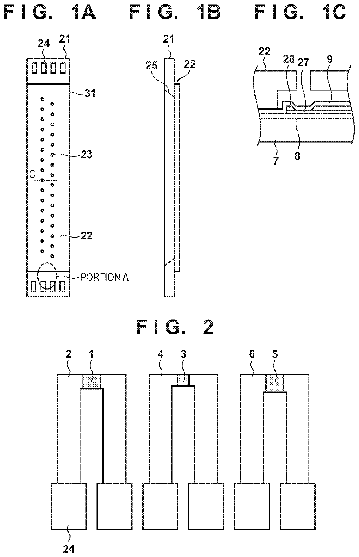
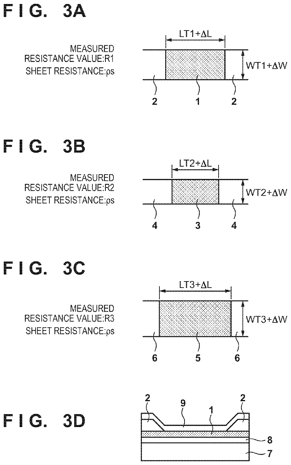
[0044]A case in which the three types of resistance monitor elements shown in FIGS. 3A to 3D are used will be described. Note that the number of resistance monitor elements is merely an example and is not limited to this number.
[0045]FIG. 3A shows a resistor 1 as a first resistance monitor element and electrodes 2 connected to this. The width of the resistor 1 is represented by WT1+ΔW, and the length is represented by LT1+ΔL. WT1 and LT1 are the design value of the width and the design value of the length of the first resistance monitor element. In addition, ΔW and ΔL are the deviation amount of the width and the deviation amount of the length of the resistor from the design values at the time of formation. The sheet resistance value of the resistor 1 is ρs, and the resistance value of the first resistance monitor element is R1. Note that the width of the resistor 1 is the length of the resistor 1 in the direction orthogonal to the direction in which a current flows in the resistor ...
second embodiment
[0087]FIGS. 8A, 8B, 8C, and 8D are views showing examples of the arrangements of resistance monitor elements according to the second embodiment of the present invention. This is an example of a case in which the layers of the resistance elements are made flat using a planarization technique.
[0088]FIG. 8A shows a resistor 11 serving as a first resistance monitor element, electrodes 12, and a plurality of vias 13 that electrically connect the resistor 11 and the electrodes 12. FIG. 8B shows a resistor 14 serving as a second resistance monitor element, electrodes 15, and the vias 13 that electrically connect the resistor 14 and the electrodes 15. FIG. 8C shows a resistor 16 serving as a third resistance monitor element, electrodes 17, and the vias 13 that electrically connect the resistor 16 and the electrodes 17. Note that in the resistance monitor element according to this embodiment, since a current flows to a portion of the resistor located between the plurality of pairs of vias 13...
third embodiment
[0094]FIGS. 9A, 9B, and 9C are views showing examples of the arrangements of resistance monitor elements according to the third embodiment of the present invention. This is an example of a case in which the connection method for the resistors of the resistance monitor elements is changed.
[0095]FIG. 9A shows a resistor 91 serving as a first resistance monitor element, and electrodes 92 connected to the resistor 91. The width of the resistor 91 is represented by WT4+ΔW, and the length is represented by LT4+ΔL. WT4 and LT4 are the design value of the width and the design value of the length of the first resistance monitor element. In addition, ΔW and ΔL are the deviation amount of the width and the deviation amount of the length of the resistor from the design values at the time of formation. The sheet resistance value of the resistor 91 is ρs, and the resistance value of the first resistance monitor element is R4.
[0096]FIG. 9B shows resistors 93 serving as second resistance monitor el...
PUM
 Abstract
Description
Claims
Application Information
 - R&D
- Intellectual Property
- Life Sciences
- Materials
- Tech Scout
- Unparalleled Data Quality
- Higher Quality Content
- 60% Fewer Hallucinations
Browse by: Latest US Patents, China's latest patents, Technical Efficacy Thesaurus, Application Domain, Technology Topic, Popular Technical Reports.
© 2025 PatSnap. All rights reserved.Legal|Privacy policy|Modern Slavery Act Transparency Statement|Sitemap|About US| Contact US: help@patsnap.com


