Sensor device
a sensor and sensor technology, applied in the field of sensor devices, can solve problems such as contamination during device singulation, and achieve the effect of easing the singulation of the sensor devi
- Summary
- Abstract
- Description
- Claims
- Application Information
AI Technical Summary
Benefits of technology
Problems solved by technology
Method used
Image

Examples
Embodiment Construction
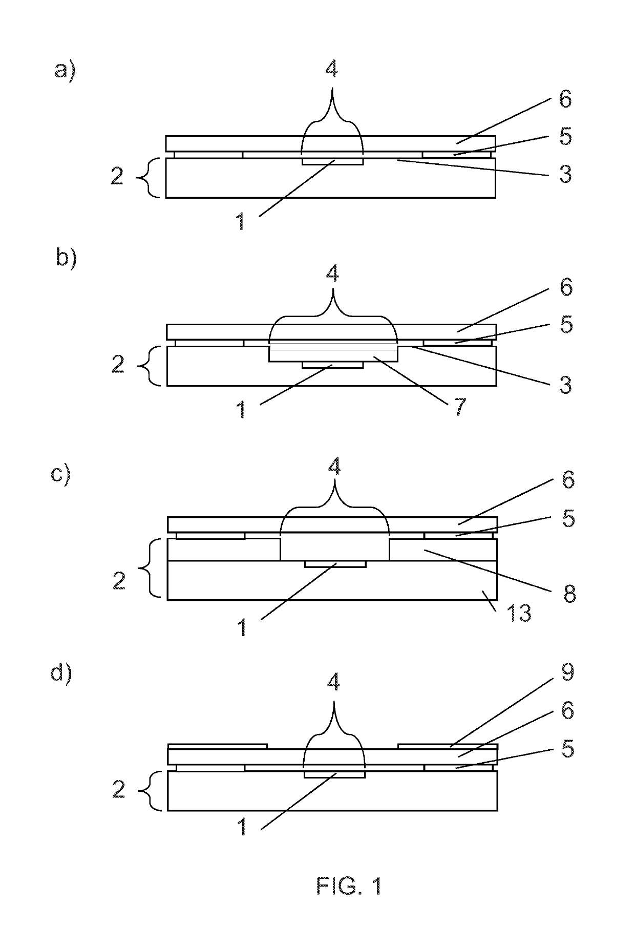
[0034]FIG. 1a) shows a schematic sectional view of a sensor device in accordance with an embodiment of the present invention. The sensor device includes a sensitive element 1, which is integrated in a support 2. In this embodiment, the support 2 is a semiconductor substrate, e.g. a silicon substrate, and it may include additional features, such as a heater structure, a suspended membrane, an integrated processing circuit, through silicon vias and solder balls. The gas to be sensed can enter the sensitive element 1 via the access opening 4 which is located in a surface 3 of the support 2. Parts of the surface 3 are covered by a layer of adhesive material 5. A venting medium 6 extends over the entire surface 3 of the support 2 and the access opening 4 and is attached to the support 2 by the layer of adhesive material 5.
[0035]FIG. 1b) shows another embodiment of a sensor device in accordance with the present invention. In this embodiment, the sensitive element 1 is located in a cavity ...
PUM
| Property | Measurement | Unit |
|---|---|---|
| thickness | aaaaa | aaaaa |
| conductive | aaaaa | aaaaa |
| thermal insulation | aaaaa | aaaaa |
Abstract
Description
Claims
Application Information
 - R&D
- Intellectual Property
- Life Sciences
- Materials
- Tech Scout
- Unparalleled Data Quality
- Higher Quality Content
- 60% Fewer Hallucinations
Browse by: Latest US Patents, China's latest patents, Technical Efficacy Thesaurus, Application Domain, Technology Topic, Popular Technical Reports.
© 2025 PatSnap. All rights reserved.Legal|Privacy policy|Modern Slavery Act Transparency Statement|Sitemap|About US| Contact US: help@patsnap.com