Static protection system using the floating and/or deflected multi-crystal silicon area and its method

一种静电放电保护、多晶硅的技术,应用在电路、晶体管、电气元件等方向,能够解决减小击穿电压困难、有效性受限、增加制造复杂度等问题,达到延迟时间、容易使用、减小损坏的效果

Active Publication Date: 2007-07-11
SEMICON MFG INT (SHANGHAI) CORP +1
View PDF0 Cites 0 Cited by
  • Summary
  • Abstract
  • Description
  • Claims
  • Application Information

AI Technical Summary

Problems solved by technology

Effective protection usually requires lowering the breakdown voltage of the I / O transistors, but reducing the breakdown voltage can be difficult
Traditionally, ESD implantation has been used to adjust the breakdown voltage, but ESD implantation usually adds manufacturing complexity, which makes the effectiveness limited

Method used


Image

  • Static protection system using the floating and/or deflected multi-crystal silicon area and its method
  • Static protection system using the floating and/or deflected multi-crystal silicon area and its method
  • Static protection system using the floating and/or deflected multi-crystal silicon area and its method

Examples


Embodiment Construction

[0022] The present invention relates to integrated circuits. More specifically, the present invention provides a system and method for electrostatic discharge (ESD) protection using floating and / or biased polysilicon regions. As an example, the invention has been applied to input / output (I / O) devices. However, it should be recognized that the invention has a much broader range of applicability.

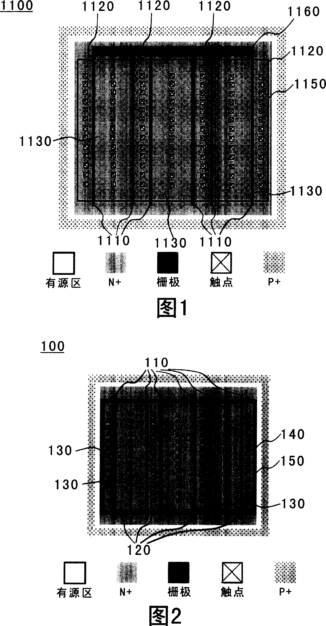
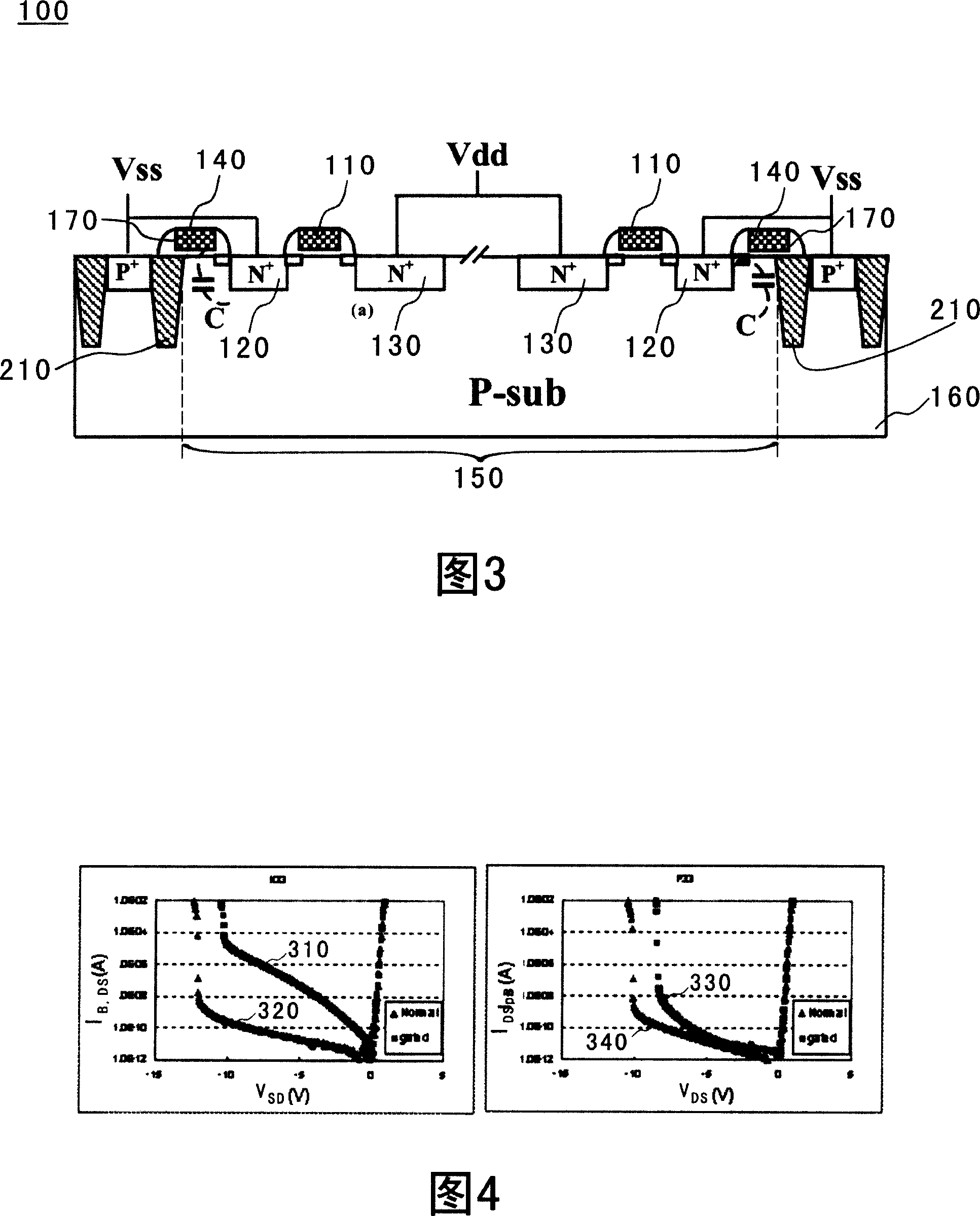
[0023] Figure 1 is a simplified conventional system for ESD protection. System 1100 includes gate region 1110 , source region 1120 , drain region 1130 , active region 1150 and polysilicon region 1160 . Gate region 1110 , source region 1120 and drain region 1130 are used to form I / O transistors in active region 1150 . The gate regions are shorted to each other via the polysilicon region 1160 , which is located entirely outside the active region 1150 . FIG. 2 is a system for electrostatic discharge protection according to an embodiment of the present invention. This diagram is mere...


PUM


Abstract

This invention discloses one static discharge protection system and method, wherein, the system comprises multiple transistor tubes composed of multiple grating areas, source electrode areas and leakage electrode areas in the source area center of underlay near isolation area in the underlay; the system comprises multi-silicon area isolated from dielectric layer and underlay; the multi-silicon area partly is in source area.

Description

technical field [0001] The present invention relates to integrated circuits. More specifically, the present invention provides a system and method for electrostatic discharge (ESD) protection using floating and / or biased polysilicon regions. As an example, the invention has been applied to input / output (I / O) devices. However, it should be recognized that the invention has a much broader range of applicability. Background technique [0002] Integrated circuits, or "ICs," have grown from a handful of interconnected devices fabricated on a single silicon wafer to millions of devices. Current ICs offer performance and complexity far beyond what was originally envisioned. In order to achieve progress in complexity and circuit density (i.e., the number of devices that can be packaged on a given chip area), the minimum device feature size (also known as device "geometry") accompanies the development of each generation of integrated circuits and become smaller. The feature size...

Claims


Application Information

Patent Timeline
Patent Type & Authority Applications(China)
IPC IPC(8): H01L27/02H01L23/60
CPCH01L27/0266
Inventor 苏鼎杰郑敏祺廖金昌黄俊诚
Owner SEMICON MFG INT (SHANGHAI) CORP
Why Eureka
Try Eureka