Optical device and its making method
An optical device and optical technology, applied in the direction of optics, optical components, light guides, etc., can solve the problem of increased transmission loss
- Summary
- Abstract
- Description
- Claims
- Application Information
AI Technical Summary
Problems solved by technology
Method used
Image

Examples
example 1
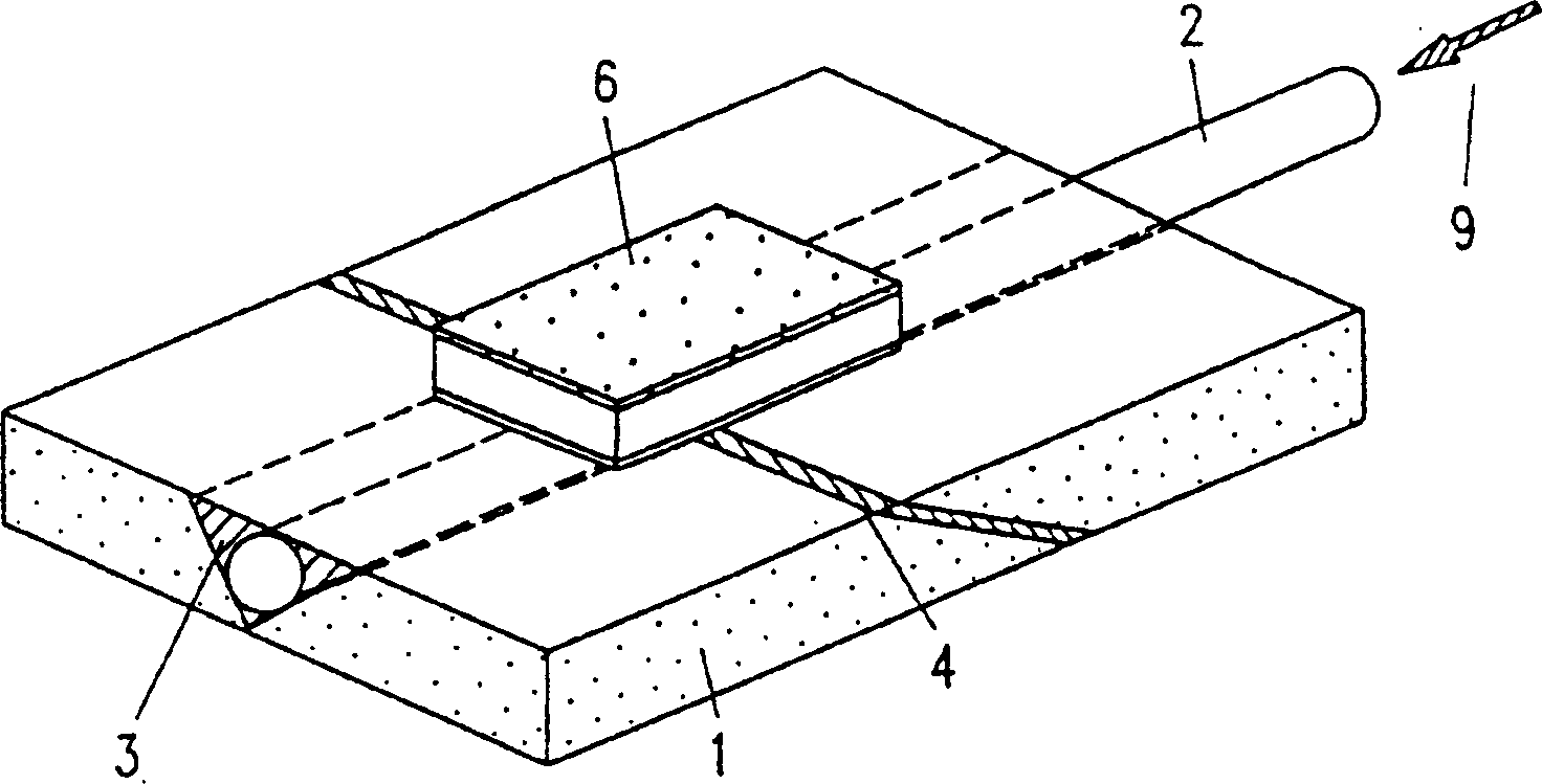
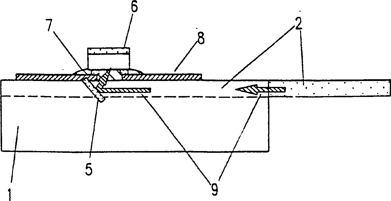
[0158] First, see Figure 1A and 1B , a first example of an optical device according to the present invention will be described. Figure 1A is a perspective view showing the uppermost part of a first example of an optical device (light receiving module) of this example, Figure 1B is a cross-sectional view of the optical device taken along an optical fiber.
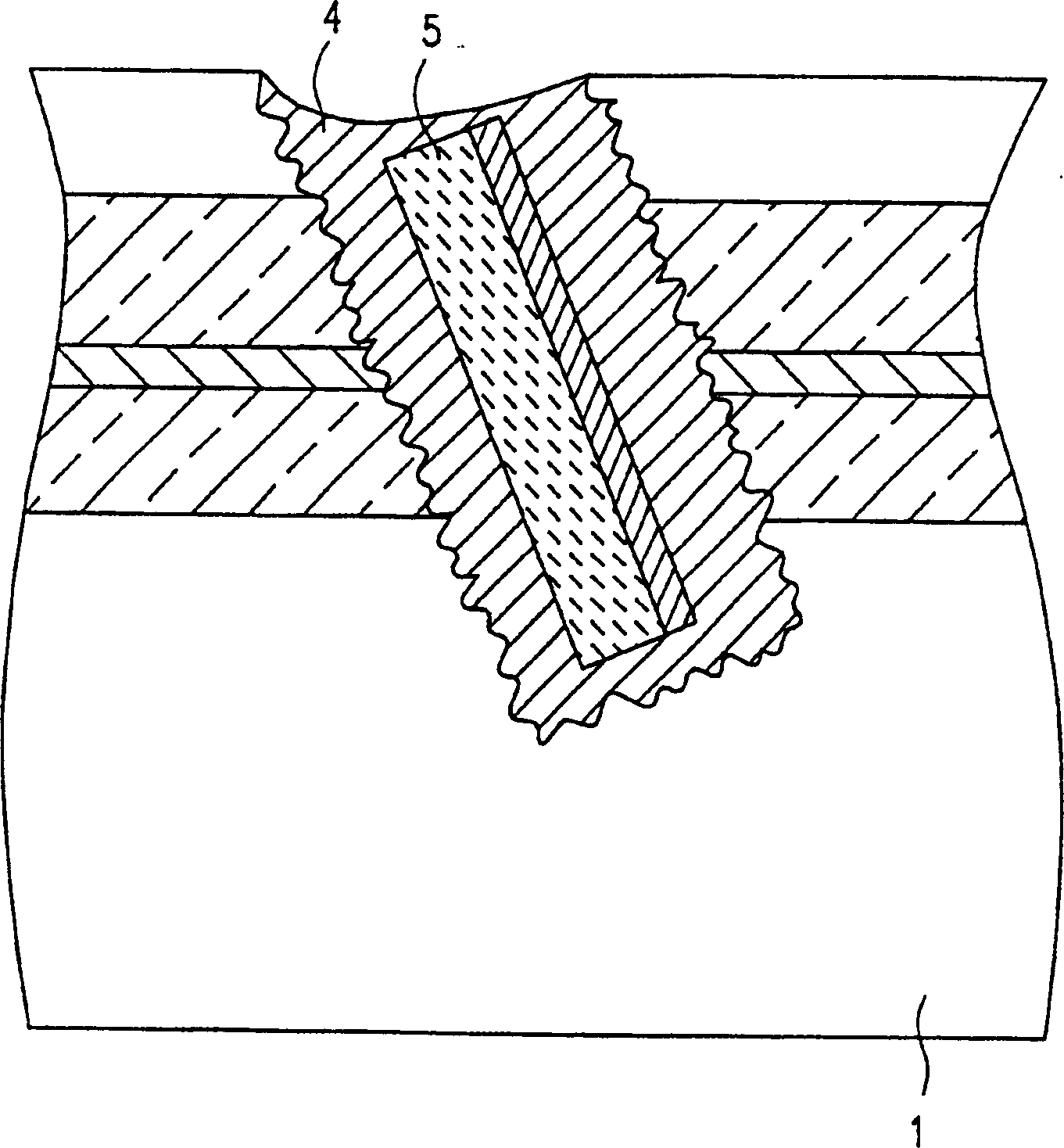
[0159] The optical device is to use a glass substrate 1 (thickness 2 mm; 5 mm long and 3 mm wide) with a V-groove (first groove) 3 formed on a flat upper surface of the substrate 1 with a diameter of about 130 μm. depth. An optical fiber 2 having an outer diameter of 125 μm is placed in the V-groove 3, and a parallel groove (second groove) 4 is formed on the upper surface of the glass substrate 1 so as to cross the optical fiber 2 diagonally. (relative to its optical axis). Due to the parallel groove 4 a gap is formed diagonally in the optical fiber 2 so that the optical fiber 2 is separated into two parts spatially ...
example 2
[0189] Next, see Figure 5 , a second example of the light receiving device according to the present invention will be described. Figure 5 is a cross-sectional view of a light-receiving optical device for receiving signal light with a wavelength λ1 of 1.55 μm and an optical signal with a wavelength λ2 of 1.31 μm. In the following description, the same elements as those in the previous examples are denoted by the same reference numerals, and detailed descriptions thereof are omitted.
[0190] Such as Figure 5 As described in , two parallel grooves (groove width: about 100 μm) were formed in the glass substrate 1 to form a predetermined angle with respect to the optical axis of the optical fiber 2 . In this example, the angles formed by the parallel grooves and the optical axis are equal. However, they can be different from each other.
[0191] As shown in Example 1, the optical fiber 2 is fixed with resin in a groove formed on the upper surface of the glass substrate 1 . ...
example 3
[0205] Next, see Figure 7A , 7B and 8, describe a third example of a device of the present invention.
[0206] In the device of this example, a hybrid integrated on a substrate such as Figure 5 A photodetector and an electrical amplifier that receive an optical signal with two wavelengths are shown in . Figure 7A It is an equivalent circuit representing a part of the circuit of the device of this example; FIG. 7B is a schematic perspective view thereof; Figure 7C for its plan view.
[0207] As shown in Figure 7B, on the substrate 1 is formed as Figure 5 The photodetectors 13 and 14 are shown in . As described in Example 2, the photodetectors 13 and 14 respectively detect signal light in a selected wavelength band among the light propagating through the optical fiber 2 embedded in a groove (not shown).
[0208] The photodetector is in Figure 7A is represented by the symbol of a photodiode. When the photodetector receives signal light, the potential of a portion bet...
PUM
 Abstract
Description
Claims
Application Information
 - R&D Engineer
- R&D Manager
- IP Professional
- Industry Leading Data Capabilities
- Powerful AI technology
- Patent DNA Extraction
Browse by: Latest US Patents, China's latest patents, Technical Efficacy Thesaurus, Application Domain, Technology Topic.
© 2024 PatSnap. All rights reserved.Legal|Privacy policy|Modern Slavery Act Transparency Statement|Sitemap