Prodn. of organic electrical lighting device
An electroluminescent device, organic technology, applied in electroluminescent light sources, semiconductor/solid-state device manufacturing, electro-solid-state devices and other directions, can solve the problem of pixel size limitation, high operating voltage, inapplicability, etc., to achieve high cancellation costs, The effect of improving yield and improving resolution
- Summary
- Abstract
- Description
- Claims
- Application Information
AI Technical Summary
Problems solved by technology
Method used
Image
Examples
Embodiment 1
[0052] Preparation of OLED-displays with photosensitive first layer
[0053] The process of preparing the display is as follows:
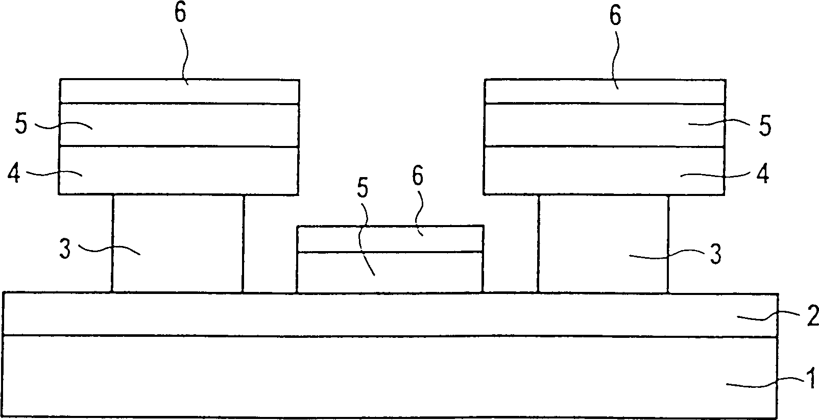
[0054] 1. Structuring of a flat glass plate coated with indium-tin-oxide (ITO) by photographic methods followed by wet chemical etching to form parallel circuits with a width of about 200 μm and an intermediate space of about 50 μm . The circuits are each about 2 cm long and optionally contain attachments for contacting at their outer ends. The photoresist used during structuring is then completely removed.
[0055] 2. Heat the glass plate at 250°C for about 1 hour, and then spin-coat commercial photosensitive adhesive based on polyglutarimide (coating at 700 rpm for 10 seconds, and at 4000 Centrifuge the gel for 30 seconds at 1 rpm). The obtained layer was dried on a hot plate at 250° C. for 170 seconds. Then use light with a wavelength of 248nm (polychromatic) at 1000mJ / cm 2 The amount of light for spot exposure. Thereafter, a commercial p...
Embodiment 2
[0060] Fabrication of OLED displays with non-photosensitive first layer
[0061] The process of preparing the display is as follows:
[0062] 1. A glass plate coated over the entire surface with indium-tin-oxide (ITO) is structured by means of photographic methods and wet-chemical etching to produce parallel circuits with a width of approximately 200 μm and a spacing of approximately 50 μm. The circuits are each approximately 2 cm long and may have attachments for contacting at their outer ends. The photoresist used in structuring is completely removed.
[0063]2. Heat the glass plate at 250°C for about 1 hour, then spin coat a commercial non-photosensitive polyimide by centrifugation at 5000 rpm for 30 seconds. The obtained layer was dried on a hot plate at 100° C. for 90 seconds (layer thickness: 10 μm). Thereafter, a phenolic resin / diazoquinone (diluted in a ratio of 10:1 with (1-methoxy-2-propyl)-acetate) was spin-coated at 2000 rpm. Commercial photoresist takes about ...
Embodiment 3
[0068] Preparation of organic light-emitting diodes according to the prior art and the present invention
[0069] Two samples were prepared, one using a common mask (sample A) and the other using the method of the present invention (sample B).
[0070] Sample A:
[0071] Circuits 2 mm wide were produced using known photographic methods on indium-tin-oxide-coated glass plates. Thereafter, at 10 -5 A layer of N,N'-bis(3-methyl-phenyl)-N,N'-bis(phenyl)-benzidine (m-TPD) was deposited with a thickness of 135 nm under mbar pressure. layer. Without breaking the vacuum, a quinoline-aluminum(III)-salt (Alq) layer was then deposited to a thickness of 65 nm. Here, thermal evaporation ("physical vapor deposition", PVD) is employed (deposition rate: respectively 0.2 nm / s). A layer of magnesium with a thickness of 100 nm and then a layer of silver with a thickness of 100 nm was deposited using a mask, resulting in a 2 nm wide metal circuit (pressure: 10 -5 mbar, deposition rate: 1 nm...
PUM
| Property | Measurement | Unit |
|---|---|---|
| width | aaaaa | aaaaa |
| thickness | aaaaa | aaaaa |
| Evaporation rate | aaaaa | aaaaa |
Abstract
Description
Claims
Application Information
 - Generate Ideas
- Intellectual Property
- Life Sciences
- Materials
- Tech Scout
- Unparalleled Data Quality
- Higher Quality Content
- 60% Fewer Hallucinations
Browse by: Latest US Patents, China's latest patents, Technical Efficacy Thesaurus, Application Domain, Technology Topic, Popular Technical Reports.
© 2025 PatSnap. All rights reserved.Legal|Privacy policy|Modern Slavery Act Transparency Statement|Sitemap|About US| Contact US: help@patsnap.com


