


Quick Research
Generate reliable direction feasibility study reports for your R&D in just a few steps.

Technical Q&A
Discover and master advanced knowledge NOW. Basics, ideas, possibilities, all at once.

Find Solutions
As an expert in R&D theories, this can generate solutions to your technical problems instantly.

Evaluate Feasibility
Analyze your overall solution with one click, know your potential R&D risks in advance.

Monitor Landscape
Get weekly tech updates, stay abreast of the latest tech innovations and key insights.
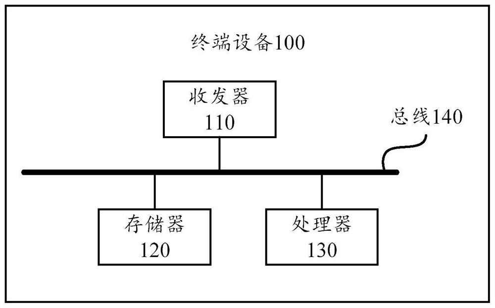
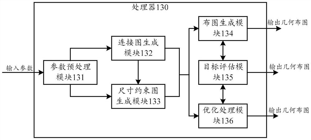
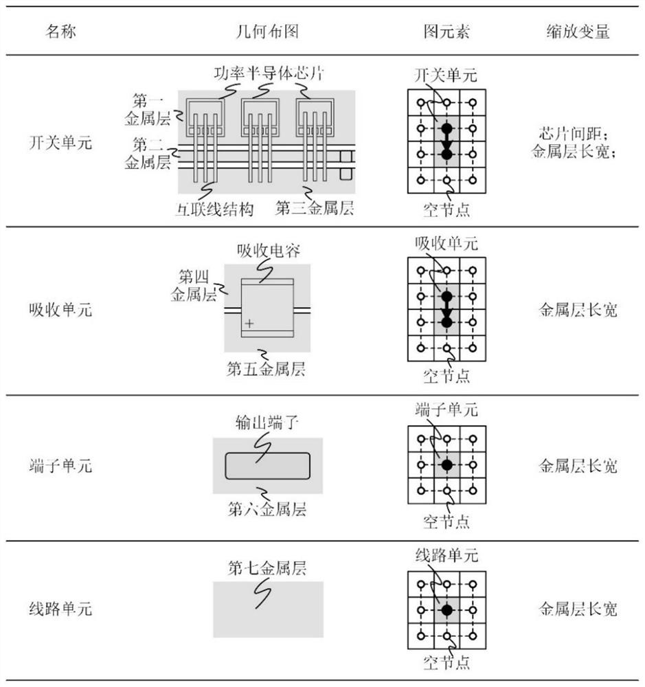
Substrate design method and device of power module and terminal equipment
A power module and substrate technology, which is applied in design optimization/simulation, computer-aided design, calculation, etc., can solve problems such as time-consuming and labor-intensive, substrate dependence on labor, difficult substrate reuse, etc.
- Summary
- Abstract
- Description
- Claims
- Application Information
AI Technical Summary
Problems solved by technology
Method used
Image

Examples
Embodiment Construction
[0067] The technical solutions in the embodiments of the present application will be described below with reference to the drawings in the embodiments of the present application.
[0068] The term "and / or" in this article is an association relationship describing associated objects, which means that there can be three relationships, for example, A and / or B can mean: A exists alone, A and B exist simultaneously, and B exists alone These three situations. The symbol " / " in this document indicates that the associated object is an or relationship, for example, A / B indicates A or B.
[0069] The terms "first" and "second" and the like in the specification and claims herein are used to distinguish different objects, not to describe a specific order of objects. For example, the first response message and the second response message are used to distinguish different response messages, rather than describing a specific order of the response messages.
[0070] In the embodiments of th...
PUM
 Abstract
Description
Claims
Application Information
 - R&D Engineer
- R&D Manager
- IP Professional
- Industry Leading Data Capabilities
- Powerful AI technology
- Patent DNA Extraction
Browse by: Latest US Patents, China's latest patents, Technical Efficacy Thesaurus, Application Domain, Technology Topic, Popular Technical Reports.
© 2024 PatSnap. All rights reserved.Legal|Privacy policy|Modern Slavery Act Transparency Statement|Sitemap|About US| Contact US: help@patsnap.com