


Quick Research
Generate reliable direction feasibility study reports for your R&D in just a few steps.

Technical Q&A
Discover and master advanced knowledge NOW. Basics, ideas, possibilities, all at once.

Find Solutions
As an expert in R&D theories, this can generate solutions to your technical problems instantly.

Evaluate Feasibility
Analyze your overall solution with one click, know your potential R&D risks in advance.

Monitor Landscape
Get weekly tech updates, stay abreast of the latest tech innovations and key insights.
Preparation method of PCB (Printed Circuit Board) and PCB
A conductive section and core board technology, which is applied in printed circuit manufacturing, multilayer circuit manufacturing, printed circuit dielectric, etc., can solve problems affecting PCB preparation, poor compatibility, poor material compatibility, etc., achieve good compatibility and eliminate signal transmission Effect, the effect of simple preparation method
- Summary
- Abstract
- Description
- Claims
- Application Information
AI Technical Summary
Problems solved by technology
Method used
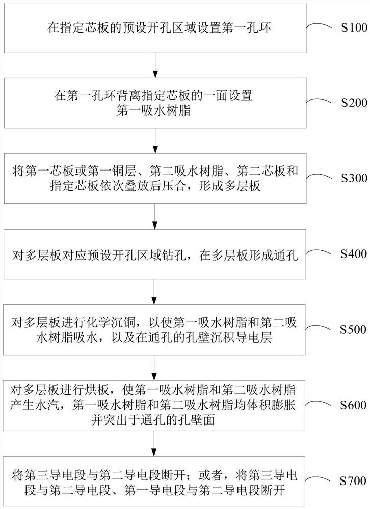
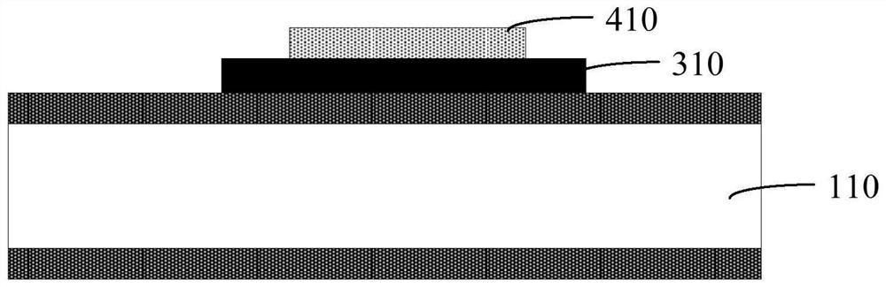
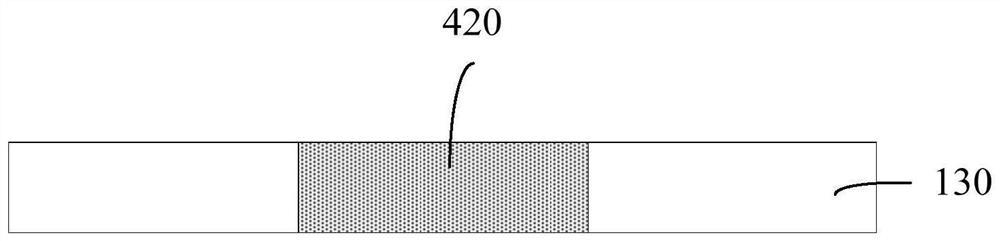
Image

Examples
Embodiment Construction
[0051] The following will clearly and completely describe the technical solutions in the embodiments of the present invention with reference to the accompanying drawings in the embodiments of the present invention. Obviously, the described embodiments are only part of the embodiments of the present invention, not all of them. Based on the embodiments of the present invention, all other embodiments obtained by persons of ordinary skill in the art without creative efforts fall within the protection scope of the present invention.
[0052] It should be noted that if there is a directional indication (such as up, down, left, right, front, back...) in the embodiment of the present invention, the directional indication is only used to explain the position in a certain posture (as shown in the accompanying drawing). If the specific posture changes, the directional indication will also change accordingly.
[0053] In addition, if there are descriptions involving "first", "second" and ...
PUM
 Abstract
Description
Claims
Application Information
 - R&D Engineer
- R&D Manager
- IP Professional
- Industry Leading Data Capabilities
- Powerful AI technology
- Patent DNA Extraction
Browse by: Latest US Patents, China's latest patents, Technical Efficacy Thesaurus, Application Domain, Technology Topic, Popular Technical Reports.
© 2024 PatSnap. All rights reserved.Legal|Privacy policy|Modern Slavery Act Transparency Statement|Sitemap|About US| Contact US: help@patsnap.com