Display panel and display device

A technology of display panel and display area, used in static indicators, instruments, nonlinear optics, etc., and can solve problems such as adverse effects on imaging quality

Active Publication Date: 2021-09-10
XIAMEN TIANMA MICRO ELECTRONICS
View PDF5 Cites 0 Cited by
  • Summary
  • Abstract
  • Description
  • Claims
  • Application Information

AI Technical Summary

Problems solved by technology

[0003] However, based on the structure of the existing liquid crystal display panel, when the external ambient light enters, there will be a relatively obvious diffraction phenomenon, which will have a negative impact on the image quality.

Method used


Image

  • Display panel and display device
  • Display panel and display device
  • Display panel and display device

Examples


Embodiment Construction

[0057] The present invention will be further described in detail below in conjunction with the accompanying drawings and embodiments. It should be understood that the specific embodiments described here are only used to explain the present invention, but not to limit the present invention. In addition, it should be noted that, for the convenience of description, only some structures related to the present invention are shown in the drawings but not all structures.

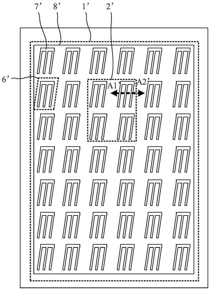
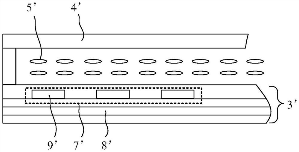
[0058] Such as figure 1 and figure 2 as shown, figure 1 is a top view of a liquid crystal display panel in the prior art, figure 2 for figure 1 In the cross-sectional view along the direction A1'-A2', the display area 1' of the liquid crystal display panel includes a high light transmission area 2', and the high light transmission area 2' is provided with a camera module. The liquid crystal display panel includes an array substrate 3' and a color filter substrate 4' disposed opposite to each other, and liqui...


PUM

PropertyMeasurementUnit
heightaaaaaaaaaa
electrical resistanceaaaaaaaaaa

Abstract

The invention provides a display panel and a display device. The display panel comprises a first display area and a second display area, and the light transmittance of the first display area is larger than that of the second display area; the first display area comprises a plurality of first sub-pixels, at least part of the first sub-pixels comprise electrode groups, and the electrode groups comprise first electrodes and second electrodes; in the first direction, the orthographic projection of the first electrode and the orthographic projection of the second electrode are at least partially overlapped, and the first direction is parallel to the light emitting surface of the display panel; in the shooting stage, the voltage difference between the first electrode and the second electrode is greater than zero volt; and the phase property of the clamping pressure between the first electrode and the second electrode is reversed along with the frame. The invention provides a display panel and a display device so as to reduce the influence of a diffraction phenomenon on the imaging quality.

Description

technical field [0001] The present invention relates to the field of display technology, in particular to a display panel and a display device. Background technique [0002] For a display panel with a camera function, in order to increase the screen-to-body ratio of the panel, a high light transmittance area is usually set in the display area of ​​the panel, and a camera component is arranged in the high light transmittance area. Taking the liquid crystal display panel as an example, when the panel is taking pictures, the liquid crystal molecules in the high light transmission area rotate under the action of the electric field formed by the pixel electrode and the common electrode, and the external ambient light enters the camera module through the liquid crystal molecules, realizing The external ambient light is collected to realize imaging. [0003] However, based on the structure of the existing liquid crystal display panel, when the external ambient light enters, relati...

Claims


Application Information

Patent Timeline
Patent Type & Authority Applications(China)
IPC IPC(8): G02F1/1343G02F1/133G02F1/1362G09G3/36
CPCG02F1/134309G02F1/134345G02F1/13306G02F1/136286G09G3/3607G09G3/3696G02F1/13439G02F1/133776G09G2310/0297
Inventor 关琳燕王海亮李雅缨王伟鹏许素霞李俊谊
Owner XIAMEN TIANMA MICRO ELECTRONICS
Why Eureka
Try Eureka