
Manufacturing method of isolation structure, dac device and manufacturing method thereof

A manufacturing method and isolation structure technology, applied in semiconductor/solid-state device manufacturing, semiconductor devices, electrical components, etc., can solve problems affecting device performance, changing circuit characteristics, reducing the range of active regions, etc., to achieve increased integration density, The effect of improving device performance

Active Publication Date: 2021-02-12
晶芯成(北京)科技有限公司
View PDF10 Cites 0 Cited by
  • Summary
  • Abstract
  • Description
  • Claims
  • Application Information

AI Technical Summary

Problems solved by technology

Wherein, the width of the top of the isolation structure 105 is relatively large, resulting in a reduction in the range of the active area on the surface of the substrate 100, which will reduce the integration density of devices on the substrate 100
In addition, due to the small width of the bottom of the isolation structure 105, the area between the well region between the isolation structures 105 and the substrate below is relatively large, which easily causes a more obvious body effect in the device, and the floating body effect It will affect the value of the threshold voltage (Vt) of the device, change the circuit characteristics, and then affect the performance of the device

Method used


Image

  • Manufacturing method of isolation structure, dac device and manufacturing method thereof
  • Manufacturing method of isolation structure, dac device and manufacturing method thereof
  • Manufacturing method of isolation structure, dac device and manufacturing method thereof

Examples


Embodiment Construction

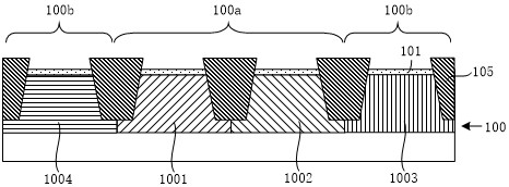
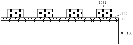
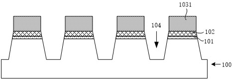
[0042] The manufacturing method of the isolation structure, the DAC device and the manufacturing method thereof proposed by the present invention will be further described in detail below in conjunction with the accompanying drawings and specific embodiments. The advantages and features of the present invention will become clearer from the following description. It should be noted that all the drawings are in a very simplified form and use imprecise scales, and are only used to facilitate and clearly assist the purpose of illustrating the embodiments of the present invention.

[0043] It should be understood that although the terms "first", "second", "third" etc. are used in the following description to describe various components, regions, layers and / or sections, these components, regions, layers and / or or parts should not be defined by these terms, and these terms are only used to distinguish different components, regions, layers and / or parts. Thus, a first component, regio...


PUM

PropertyMeasurementUnit
widthaaaaaaaaaa
widthaaaaaaaaaa

Abstract

The invention provides a manufacturing method of an isolation structure, a DAC device and a manufacturing method thereof. The manufacturing method of the isolation structure includes: using a dry etching process to form a first groove on the substrate; using a wet etching process to continue etching the substrate, so that the range of the first groove below the surface of the substrate is enlarged and A second trench is obtained, the width of the bottom surface of the second trench is greater than the width of the opening; and an isolation medium is filled in the second trench to form a plurality of isolation structures, and the width of the upper surface of the isolation structure is smaller than the width of the lower surface. Since the width of the upper surface of the isolation structure is smaller than the width of the lower surface, the effective length of the active region between the isolation structures can be increased, which helps to improve the integration density of the device and the isolation effect of adjacent active regions. In the DAC device and its manufacturing method, a plurality of isolation structures are formed in the base of the DAC device, and part of the isolation structures isolate the high-voltage area and the low-voltage area, and the isolation structure is formed by the above-mentioned manufacturing method of the isolation structure.

Description

technical field [0001] The invention relates to the technical field of semiconductors, in particular to a method for manufacturing an isolation structure, a DAC device and a method for manufacturing the same. Background technique [0002] In the current semiconductor manufacturing process, an isolation structure (such as STI) is often used to limit the range of the active region and form key components of the device in the active region. However, with the development of advanced semiconductor manufacturing processes, the size of devices in integrated circuits is getting smaller and smaller, and the probability of device performance degradation or even failure due to isolation problems between adjacent active regions is getting higher and higher. For example, in some static random In access memory (SRAM) and high-voltage devices (such as data converters (DAC devices)), P wells and N wells are formed in two adjacent active regions by implantation process, and the two active re...

Claims


Application Information

Patent Timeline
Patent Type & Authority Patents(China)
IPC IPC(8): H01L21/762H01L29/06
CPCH01L21/76224H01L29/0611H01L29/0649
Inventor 许飞李庆民杨宗凯曾伟翔
Owner 晶芯成(北京)科技有限公司
Learn More