A method and device for correcting the central wavelength of an arrayed waveguide grating
An arrayed waveguide grating and center wavelength technology, applied in the field of optical communication, can solve problems such as parameter errors affecting center wavelength, phase, frequency, etc., AWG chip process defects, etc., to improve reliability, simplify steps, and achieve the effect of accurate correction
- Summary
- Abstract
- Description
- Claims
- Application Information
AI Technical Summary
Problems solved by technology
Method used
Image
Examples
Embodiment 1
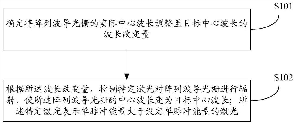
[0025] figure 1 is a schematic flowchart of a method for correcting the central wavelength of an arrayed waveguide grating provided in an embodiment of the present application, as shown in figure 1 Said, said method comprises the steps of:
[0026] S101: Determine a wavelength change amount for adjusting an actual central wavelength of the arrayed waveguide grating to a target central wavelength.
[0027] In the embodiment of the present application, the actual central wavelength of the arrayed waveguide grating can be obtained by measuring with optical measuring equipment; the target central wavelength can be the commercial standard central wavelength of the arrayed waveguide grating, or it can be set close to the above-mentioned commercial standard center wavelength according to the actual situation. wavelength of wavelength.
[0028] For the implementation of this step, for example, after the actual central wavelength is obtained by the optical measurement device, the wav...
Embodiment 2
[0054] Further illustration is made on the basis of Embodiment 1 of the present application.
[0055] In the embodiment of the present application, the operating parameters of the radiation area adjustment device are determined according to the amount of wavelength change, and the specific laser is controlled to radiate the arrayed waveguide grating according to the operating parameters of the radiation area adjustment device, thereby changing the center wavelength of the arrayed waveguide grating into the target center wavelength; certain lasers are ultrafast.
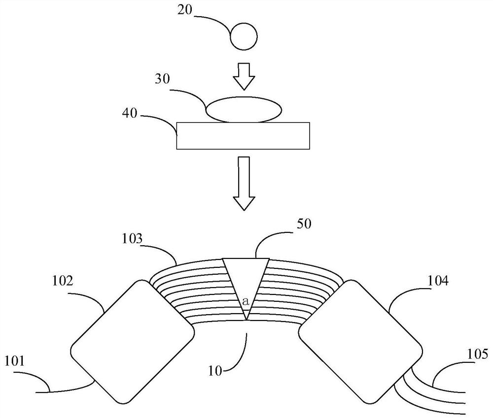
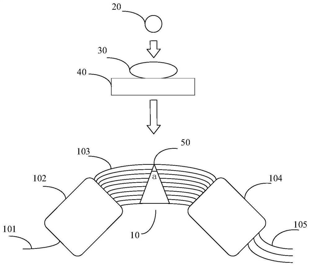
[0056] In a specific application scenario, see figure 2 , is a schematic diagram of the overall structure of a system for correcting the central wavelength of an arrayed waveguide grating provided in an embodiment of the present application, which includes: an arrayed waveguide grating 10, a light source 20 for emitting a specific laser, a lens system 30, a precision displacement platform 40, and target radiation Ar...
Embodiment 3
[0063] Further illustration is made on the basis of Embodiment 1 of the present application.
[0064] In the embodiment of the present application, the working parameters of the specific laser are determined according to the amount of wavelength change, and the specific laser is controlled to radiate the arrayed waveguide grating according to the working parameters of the specific laser, and then the central wavelength of the arrayed waveguide grating is changed to the target central wavelength; the specific laser for ultrafast lasers.
[0065] Variation of the effective refractive index of the arrayed waveguide in the target radiation area n t It is related to the parameters of the ultrafast laser. For example, when the pulse width of the ultrafast laser is greater than 200 fs, the ultrafast laser will rapidly deposit energy in the arrayed waveguide, and at the same time impact the material inside the arrayed waveguide, thereby causing The inside of the arrayed waveguide is ...
PUM
 Abstract
Description
Claims
Application Information
 - R&D
- Intellectual Property
- Life Sciences
- Materials
- Tech Scout
- Unparalleled Data Quality
- Higher Quality Content
- 60% Fewer Hallucinations
Browse by: Latest US Patents, China's latest patents, Technical Efficacy Thesaurus, Application Domain, Technology Topic, Popular Technical Reports.
© 2025 PatSnap. All rights reserved.Legal|Privacy policy|Modern Slavery Act Transparency Statement|Sitemap|About US| Contact US: help@patsnap.com


