Display panel and display device
A display panel and display area technology, applied in nonlinear optics, instruments, optics, etc., can solve problems such as irregular shape changes in high light transmission areas, affecting light transmission effect, resolution of photosensitive components, uneven wiring density, etc.
- Summary
- Abstract
- Description
- Claims
- Application Information
AI Technical Summary
Problems solved by technology
Method used
Image
Examples
Embodiment Construction
[0022] In order to make the purpose, technical solutions and advantages of the present application clearer, the following will clearly and completely describe the technical solutions in the embodiments of the present application with reference to the drawings in the embodiments of the present application.
[0023] In the prior art, for a screen with a full screen, a photosensitive component such as a camera is installed in the display area of the screen to realize functions such as a front camera. The interior of the light area is filled with liquid crystal and other substances, so as to maximize the realization of a full screen.
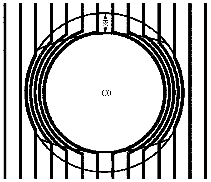
[0024] See figure 1 ,Such as figure 1 The wiring density shown in the first area of the non-display area B0 around the high light transmittance area C0 is relatively small, and the wiring density in the second area of the non-display area B0 is relatively high. It can support the substrate in the display panel together with the support colum...
PUM
 Abstract
Description
Claims
Application Information
 - R&D
- Intellectual Property
- Life Sciences
- Materials
- Tech Scout
- Unparalleled Data Quality
- Higher Quality Content
- 60% Fewer Hallucinations
Browse by: Latest US Patents, China's latest patents, Technical Efficacy Thesaurus, Application Domain, Technology Topic, Popular Technical Reports.
© 2025 PatSnap. All rights reserved.Legal|Privacy policy|Modern Slavery Act Transparency Statement|Sitemap|About US| Contact US: help@patsnap.com


