Two-dimensional heterojunction photovoltaic cell
A two-dimensional heterojunction and photovoltaic cell technology, applied in photovoltaic power generation, circuits, electrical components, etc., can solve problems such as weak light absorption, and achieve the effects of reduced spontaneous radiation loss, enhanced light absorption, and increased efficiency
- Summary
- Abstract
- Description
- Claims
- Application Information
AI Technical Summary
Problems solved by technology
Method used
Image
Examples
Embodiment 1
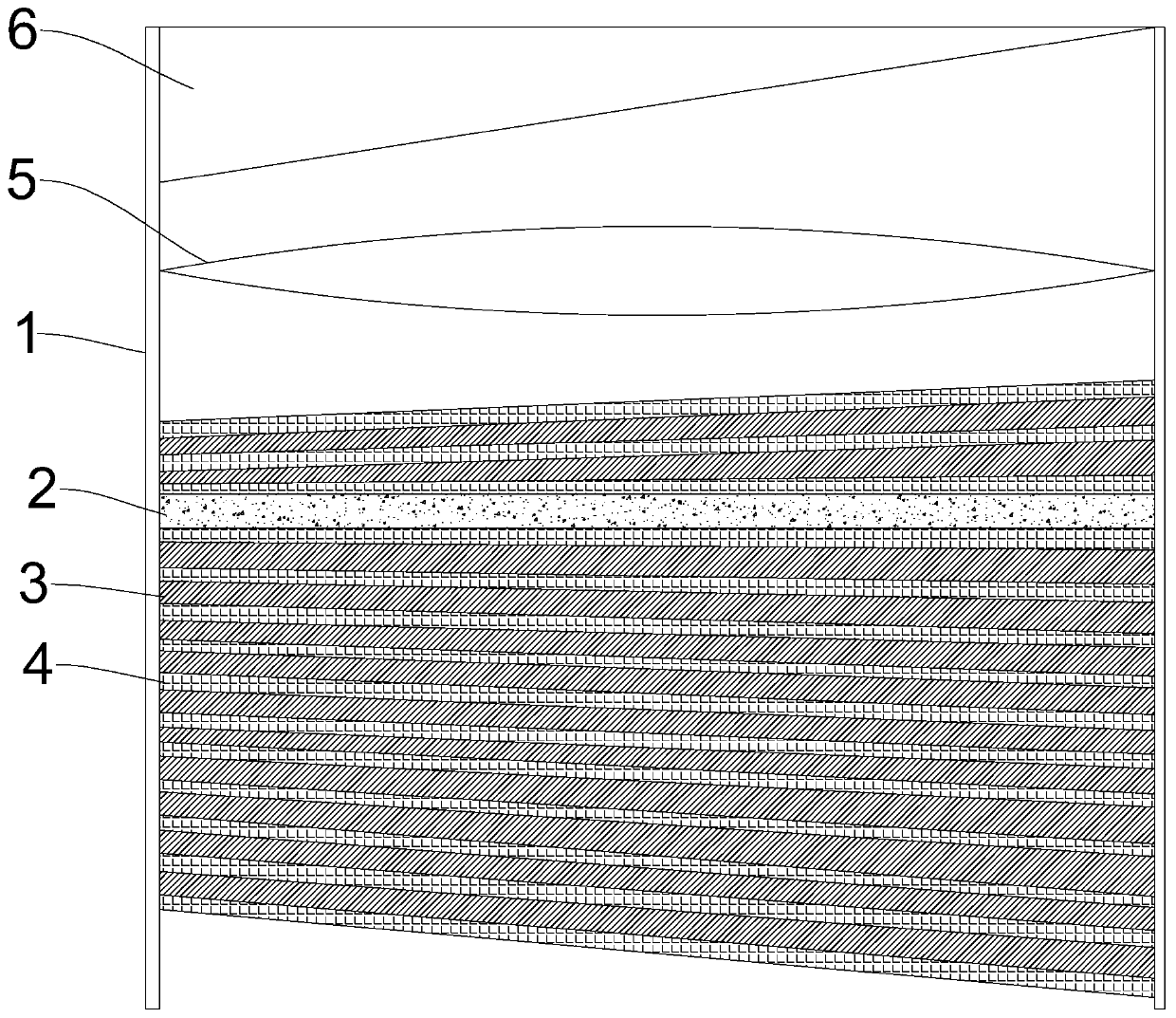
[0036] like figure 1 As shown, this embodiment provides a two-dimensional heterojunction photovoltaic cell, including a fixed layer 1, a two-dimensional material heterojunction 2 and an optical microcavity, the two-dimensional material heterojunction 2 is arranged in the optical microcavity, and the optical microcavity Both ends of the cavity are fixedly connected to the fixed layer 1, and the optical microcavity is used to reflect sunlight multiple times, so that the two-dimensional material heterojunction 2 absorbs sunlight multiple times, and the two-dimensional material heterojunction 2 absorbs photons in sunlight And converted to electrical energy output;
[0037] Specifically, the optical microcavity is a photonic crystal with a defect layer, and the two-dimensional material heterojunction 2 is located in the defect layer of the photonic crystal with a defect layer. Since the interior of the photonic crystal with a defect layer has different refractive indices, different...
Embodiment 2
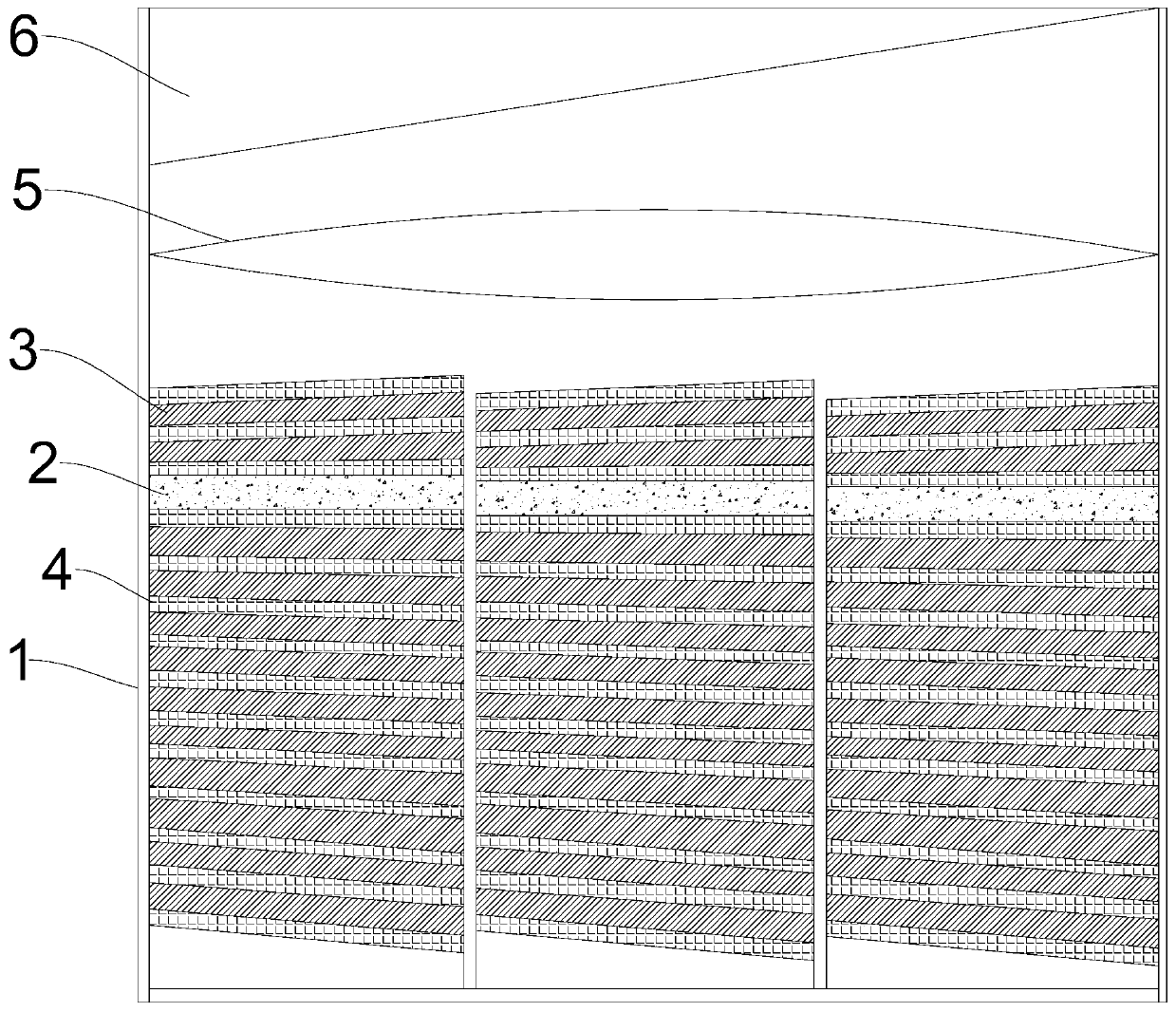
[0043] like figure 2 As shown, this embodiment also provides a two-dimensional heterojunction photovoltaic cell. The difference between this embodiment 2 and embodiment 1 is that there are three two-dimensional material heterojunctions 2 and photonic crystals containing defect layers, Distributed side by side and fixedly connected on the fixed layer 1, distributed in a side-by-side array, three photonic crystals with defect-containing layers and two-dimensional material heterojunction 2 arranged side by side in a side-by-side distribution are all arranged on the vertical side of the Fresnel convex lens 5 Directly below, the sunlight gathered by the Fresnel convex lens 5 enters the three photonic crystals containing defect layers, and the three photonic crystals containing defect layers arranged side by side and the two-dimensional material heterojunction 2 can reduce the heat dissipation. Loss, improve the conversion efficiency of the cell, because the spontaneous emission so...
PUM
 Abstract
Description
Claims
Application Information
 - R&D
- Intellectual Property
- Life Sciences
- Materials
- Tech Scout
- Unparalleled Data Quality
- Higher Quality Content
- 60% Fewer Hallucinations
Browse by: Latest US Patents, China's latest patents, Technical Efficacy Thesaurus, Application Domain, Technology Topic, Popular Technical Reports.
© 2025 PatSnap. All rights reserved.Legal|Privacy policy|Modern Slavery Act Transparency Statement|Sitemap|About US| Contact US: help@patsnap.com


