Multilayer printed circuit board and method of making multilayer printed circuit board

A multi-layer printing and circuit board technology, applied in multi-layer circuit manufacturing, printed circuit components, etc., can solve problems such as quality degradation, signal distortion, and high-frequency signal distortion

Inactive Publication Date: 2019-05-24
INVENTEC PUDONG TECH CORPOARTION +1
View PDF5 Cites 0 Cited by
  • Summary
  • Abstract
  • Description
  • Claims
  • Application Information

AI Technical Summary

Problems solved by technology

Among them, the high-frequency signal is greatly affected, and often causes signal distortion, resulting in a serious decline in quality
[0003] For example, vias are often used in multilayer printed circuit boards to connect wires between different layers. If the power layer and the ground layer are penetrated, the power noise existing on the flat layer between the power layer and the ground layer is likely to be transmitted to the connecting column, so that the high-frequency signal transmitted on the connecting column is affected and distorted

Method used


Image

  • Multilayer printed circuit board and method of making multilayer printed circuit board
  • Multilayer printed circuit board and method of making multilayer printed circuit board

Examples


Embodiment Construction

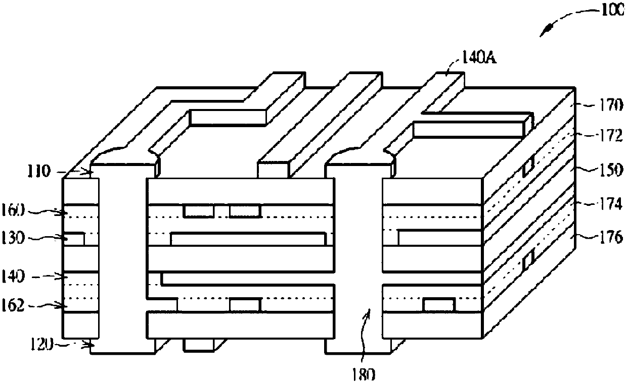
[0024] figure 1 It is a schematic diagram of a multilayer printed circuit board 100 according to an embodiment of the present invention. The multilayer printed circuit board 100 includes a first outer circuit layer 110 , a second outer circuit layer 120 , a first reference voltage layer 130 , a second reference voltage layer 140 and a high loss dielectric layer 150 .

[0025] The first reference voltage layer 130 is disposed between the first outer circuit layer 110 and the second outer circuit layer 120 , and the first reference voltage layer 130 can provide a first reference voltage. The second reference voltage layer 140 is disposed between the first reference voltage layer 130 and the second outer circuit layer 120 , and the second reference voltage layer 140 can provide a second reference voltage. In some embodiments of the present invention, the first reference voltage layer 130 and the second reference voltage layer 140 may have larger conductive planar structures, so ...


PUM


Abstract

The invention discloses a multilayer printed circuit board comprising a first external circuit layer, a second external circuit layer, a first reference voltage layer, a second reference voltage layerand a high-loss dielectric layer. The first reference voltage layer is arranged between the first external circuit layer and the second external circuit layer. The first reference voltage layer is used for providing a first reference voltage. The second reference voltage layer is arranged between the first reference voltage layer and the second external circuit layer. The second reference voltagelayer is used for providing a second reference voltage. The high-loss dielectric layer is arranged between and adjacent to the first reference voltage layer and the second reference voltage layer tosuppress the noise generated between the first reference voltage layer and the second reference voltage layer. The first reference voltage is different from the second reference voltage.

Description

technical field [0001] The present invention relates to a multilayer printed circuit board, more specifically, a multilayer printed circuit board capable of reducing signal distortion. Background technique [0002] In the prior art, a multilayer printed circuit board often includes a power layer for providing a circuit operating voltage and a ground layer for providing a reference ground voltage. Generally speaking, in order to provide a stable voltage conveniently, the power layer and the ground layer are designed as flat layers with larger areas. However, in this way, the power plane, the ground plane, and the dielectric layer between them can be regarded as plate capacitors, causing the power noise between the power plane and the ground plane to be transmitted through the dielectric layer, and will Noise is coupled elsewhere. Among them, high-frequency signals are greatly affected, and often cause signal distortion, resulting in a serious decline in quality. [0003] F...

Claims


Application Information

Patent Timeline
Patent Type & Authority Applications(China)
IPC IPC(8): H05K1/02H05K3/46
Inventor 曾淳一庄木枝丁纬范陈彦豪
Owner INVENTEC PUDONG TECH CORPOARTION
Why Eureka
Try Eureka