Display panel, display device and method for manufacturing display panel

A display panel and area technology, which is applied in the production of display devices and display panels, and in the field of display panels, can solve the problem of uneven film formation, poor dry film morphology and uniformity, device life, display effect, and solvent loss at the edge Many problems, to achieve the effect of ensuring uniformity

Active Publication Date: 2021-10-29
BOE TECH GRP CO LTD
View PDF3 Cites 0 Cited by
  • Summary
  • Abstract
  • Description
  • Claims
  • Application Information

AI Technical Summary

Problems solved by technology

During the drying process of the ink, since the solvent evaporation rate at the edge of the pixel pit is faster than that at the center, the solvent loss at the edge is more in the same time, resulting in a gradient of solute concentration between the edge and the center. The solvent in the center wants to flow to the edge, and at the same time, it drives a part of the solute to flow to the edge, which leads to the accumulation of solute at the edge. After the ink is dried and formed into a film, the edge is thicker, while the center is thinner, and the film formation is uneven.
For optoelectronic display devices, the poor morphology and uniformity of the dry film have a great impact on the life of the device and the display effect

Method used


Image

  • Display panel, display device and method for manufacturing display panel
  • Display panel, display device and method for manufacturing display panel
  • Display panel, display device and method for manufacturing display panel

Examples


Embodiment Construction

[0026] In order to further explain the technical means and effects of the present invention to achieve the intended purpose of the invention, the specific implementation of the display panel, display device and display panel manufacturing method proposed according to the present invention will be described below in conjunction with the accompanying drawings and preferred embodiments. , structure, feature and effect thereof, detailed description is as follows.

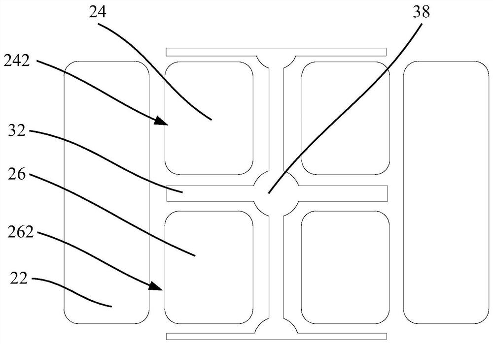
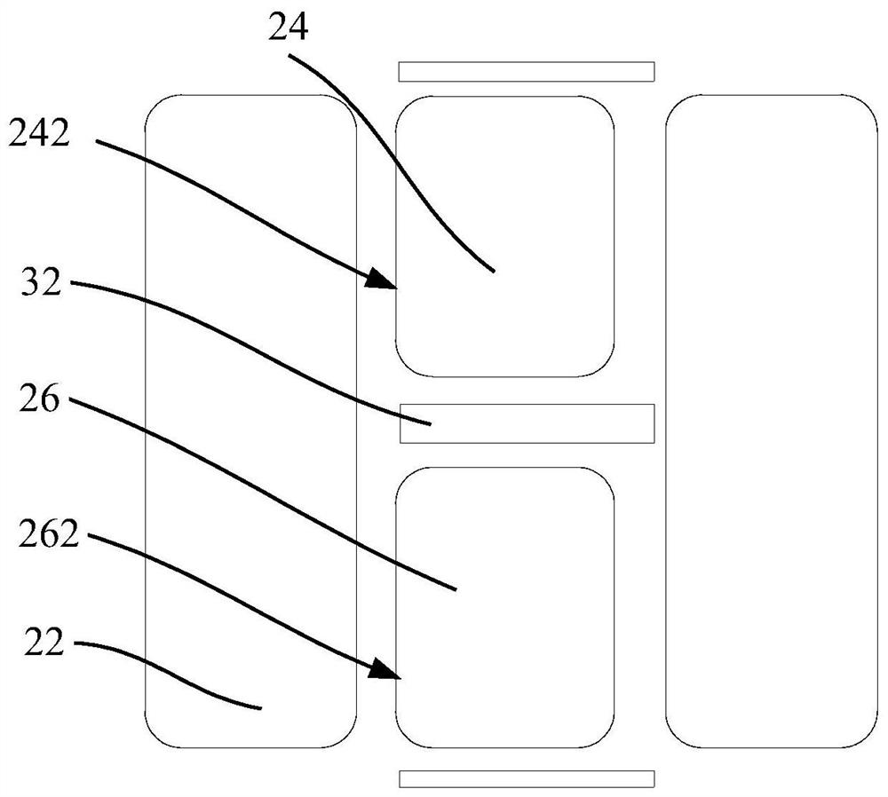
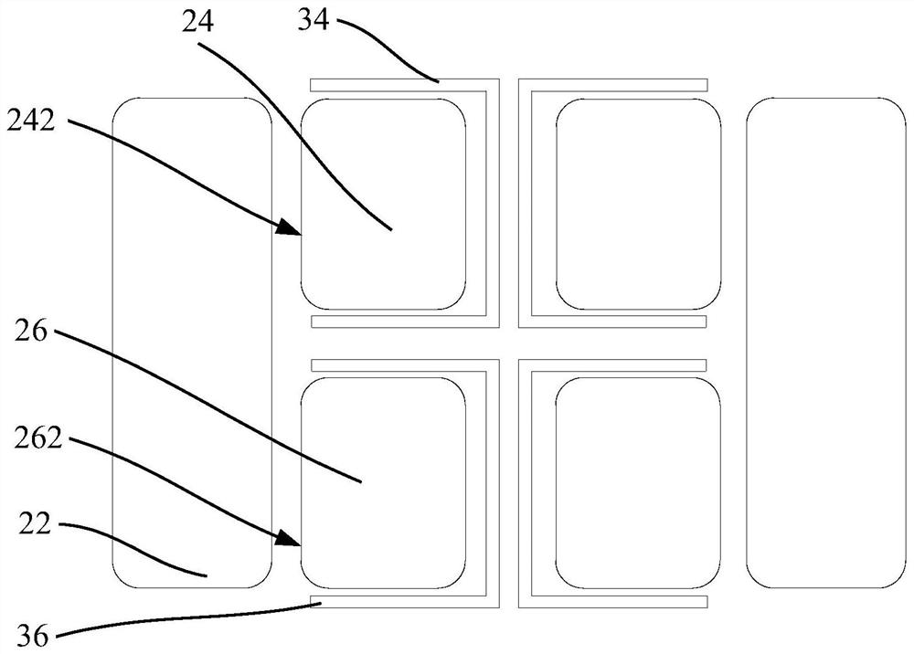
[0027] On the one hand, if Figure 1 to Figure 5 As shown, the embodiment of the present invention provides a display panel, the display panel includes: a pixel defining layer 1, a plurality of pixel pits 2 are arranged on the pixel defining layer 1, and a part or all of the pixel pits 2 of the pixel defining layer 1 The sides are provided with auxiliary grooves 3 respectively. Pixel pits 2 are arranged on the pixel defining layer 1 of the display panel. When manufacturing the pixel film 5 of the display panel, ink is ...


PUM


Abstract

The invention discloses a display panel, a display device and a manufacturing method of the display panel, which relate to the display field and achieve the purpose of making the film formation of the pixel film of the display panel more uniform. The main technical solution of the present invention is: comprising: a pixel defining layer, on which a plurality of pixel pits are arranged, and on one side of part or all of the pixel pits, the pixel defining layer is respectively provided with auxiliary grooves. The invention is mainly used in the manufacture of pixel films of display panels.

Description

technical field [0001] The present invention relates to the display field, in particular to a display panel, a display device and a manufacturing method of the display panel. Background technique [0002] Organic Light Emitting Diode (OLED) is known as a new generation of display technology. Due to its advantages of high response, high contrast, and flexibility, it is considered to have a wide range of application prospects. The inkjet printing technology in the OLED film formation technology is considered to be an important way to realize the mass production of large-size OLEDs due to its high material utilization rate. [0003] In the inkjet printing process, it is an essential step to remove the solvent through the subsequent process, so that the solute is dried to form the required film. During the drying process of the ink, since the solvent evaporation rate at the edge of the pixel pit is faster than that at the center, the solvent loss at the edge is more in the same...

Claims


Application Information

Patent Timeline
Patent Type & Authority Patents(China)
IPC IPC(8): H01L27/32H01L51/56H01L51/00
Inventor 罗程远
Owner BOE TECH GRP CO LTD
Why Eureka
Try Eureka