Display drive voltage compensation method and circuit
A technology of driving voltage and compensation method, applied in circuits, static indicators, instruments, etc., can solve problems such as leakage current Id drift, flicker, and pixel leakage speed change in AA area, and achieve the effect of solving IV curve drift
- Summary
- Abstract
- Description
- Claims
- Application Information
AI Technical Summary
Problems solved by technology
Method used
Image

Examples
Embodiment 1
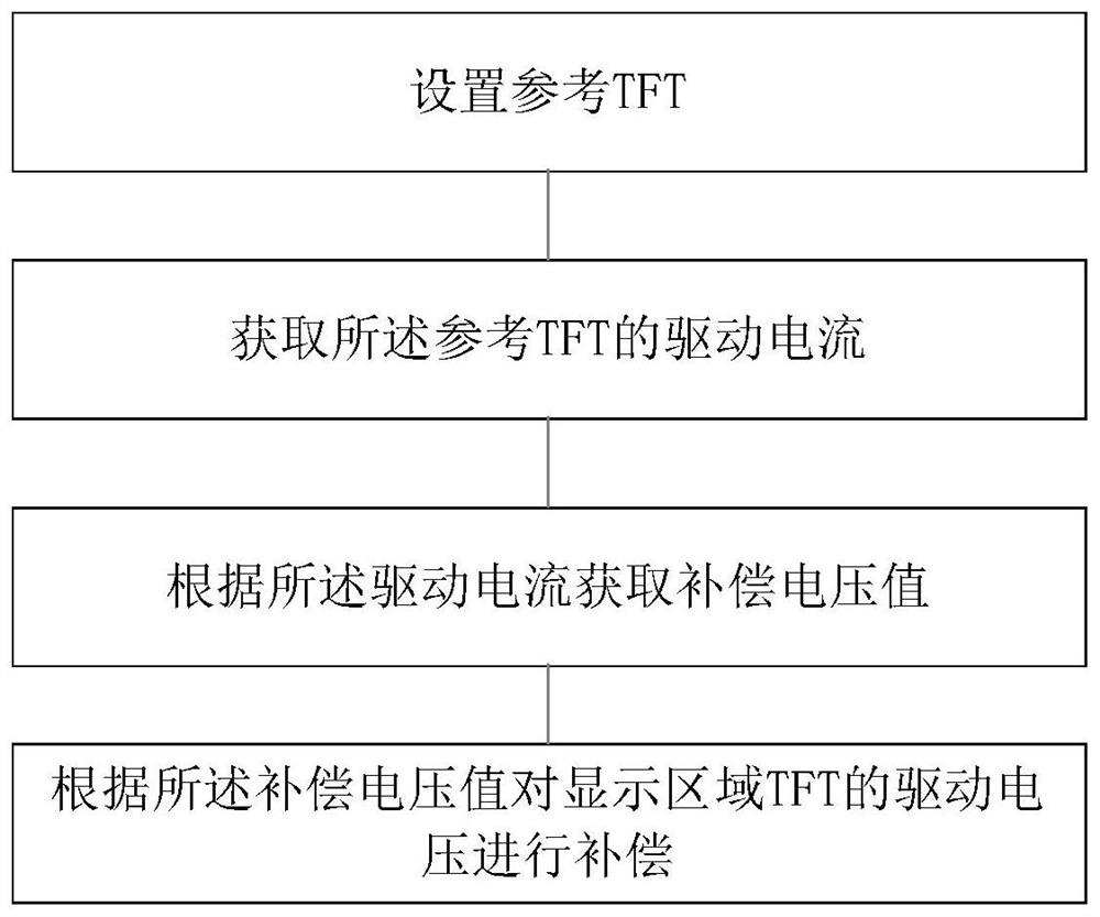
[0039] See image 3 and Figure 4 , image 3 It is a schematic flowchart of a display driving voltage compensation method provided by an embodiment of the present invention, Figure 4 A schematic diagram of a position of a reference TFT provided for an embodiment of the present invention. The voltage compensation method of this embodiment can be applied to various displays using TFTs, such as OLED displays, LCD displays, etc., and its working principle is also applicable to other types of displays, without any limitation here. Specifically, the method includes:
[0040] Set the reference TFT;
[0041] obtaining the drive current of the reference TFT;
[0042] Obtaining a compensation voltage value according to the driving current;
[0043] The driving voltage of the TFT in the display area is compensated according to the compensation voltage value.
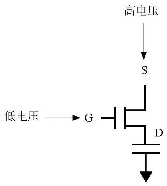
[0044] Wherein, in the display mode, the voltages of the source, drain, and gate of the reference TFT are the same as the...
Embodiment 2
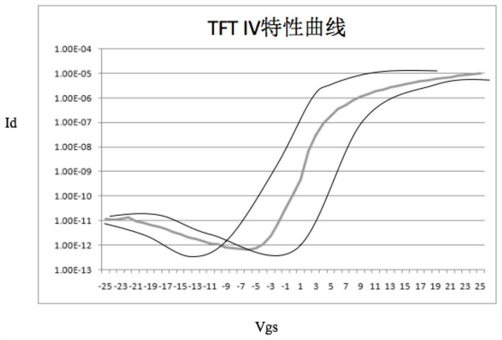
[0054] Please refer to Figure 4 to Figure 8 , Figure 4A schematic diagram of the position of a reference TFT provided by the embodiment of the present invention, Figure 5 It is a schematic diagram of the establishment principle of a compensation comparison table provided by the embodiment of the present invention, Figure 6 It is a schematic diagram of the principle of a driving voltage compensation circuit in display mode provided by an embodiment of the present invention, Figure 7 It is a schematic diagram of the principle of a driving voltage compensation circuit in the detection compensation mode provided by the embodiment of the present invention, Figure 8 It is a timing schematic diagram of a driving voltage compensation circuit provided by an embodiment of the present invention. In this embodiment, on the basis of the above-mentioned embodiments, taking reference TFTs set in the dummy area and compensating all TFTs in the AA area as an example, the driving volta...
Embodiment 3
[0083] The embodiment of the present invention introduces a driving voltage compensation circuit based on the above method. See Figure 9 and see again Figure 6 and Figure 7 , Figure 9 A block diagram of a driving voltage compensation circuit provided by an embodiment of the present invention. The compensation circuit includes: a drive current detection module 10, a compensation voltage acquisition module 20, and a compensation module 30; wherein,
[0084] The driving current detection module 10 is used to obtain the driving current drift value of the TFT in the display area, including: a reference TFT 101, a control module 102, a level conversion unit 103, a driving current detection unit 104, and an ADC 105, wherein the control module 102 is connected with the driving current respectively. The circuit detection unit 104 is connected to the level conversion unit 103 , the reference TFT 101 is respectively connected to the drive current detection unit 104 and the level ...
PUM
 Abstract
Description
Claims
Application Information
 - R&D
- Intellectual Property
- Life Sciences
- Materials
- Tech Scout
- Unparalleled Data Quality
- Higher Quality Content
- 60% Fewer Hallucinations
Browse by: Latest US Patents, China's latest patents, Technical Efficacy Thesaurus, Application Domain, Technology Topic, Popular Technical Reports.
© 2025 PatSnap. All rights reserved.Legal|Privacy policy|Modern Slavery Act Transparency Statement|Sitemap|About US| Contact US: help@patsnap.com