A defect detection method of CMOS image sensor

An image sensor and defect detection technology, which is applied in the direction of instruments, measuring devices, etc., can solve the problems of low noise floor, cannot meet the high-precision requirements in the field of machine vision, and cannot well reflect the high-precision image acquisition, so as to solve the problem of testing effect of demand

Active Publication Date: 2022-07-08
SHANGHAI INTEGRATED CIRCUIT RES & DEV CENT +1
View PDF0 Cites 0 Cited by
  • Summary
  • Abstract
  • Description
  • Claims
  • Application Information

AI Technical Summary

Problems solved by technology

[0003] However, CMOS image sensors still have many deficiencies, and sometimes cannot meet the high-precision requirements in the field of machine vision
For example, if the CMOS image sensor chip has defects of low bit and large noise floor, it cannot reflect the high precision of image acquisition.

Method used


Image

  • A defect detection method of CMOS image sensor
  • A defect detection method of CMOS image sensor
  • A defect detection method of CMOS image sensor

Examples


Embodiment Construction

[0030] The specific embodiments of the present invention will be further described in detail below with reference to the accompanying drawings.

[0031] It should be noted that, in the following specific embodiments, when describing the embodiments of the present invention in detail, in order to clearly represent the structure of the present invention for the convenience of description, the structure in the accompanying drawings is not drawn according to the general scale, and the Partial enlargement, deformation and simplification of processing are shown, therefore, it should be avoided to interpret this as a limitation of the present invention.

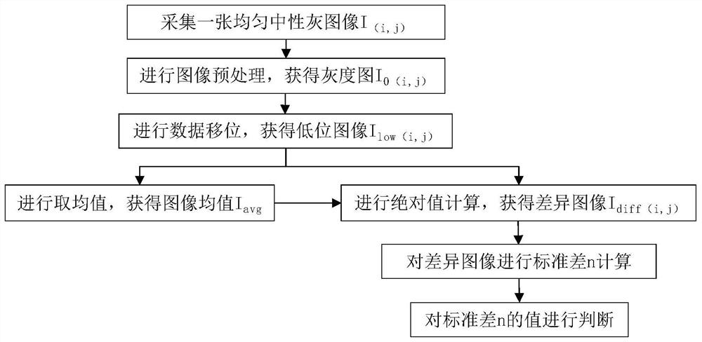
[0032] In the following specific embodiments of the present invention, please refer to figure 1 , figure 1 It is a flow chart of a defect detection method of a CMOS image sensor according to a preferred embodiment of the present invention. like figure 1 As shown, a defect detection method for a CMOS image sensor of the present in...


PUM


Abstract

The invention discloses a defect detection method of a CMOS image sensor. Perform data shift processing on each pixel value in the low-order image to obtain a low-order image; average each pixel value in the low-order image to obtain an image mean value; perform absolute value calculation between each pixel value in the low-order image and the image mean to obtain a difference image; The standard deviation is calculated for each pixel value in the difference image; when the obtained standard deviation is greater than the preset standard deviation threshold, it is determined that the CMOS image sensor chip has the defect that the low-level image noise floor exceeds the standard. The present invention can well solve the testing requirements for high-precision image sensors.

Description

technical field [0001] The present invention relates to the technical field of semiconductor testing, and more particularly, to a method for detecting defects of a CMOS image sensor used for machine vision. Background technique [0002] In recent years, CMOS image sensors have been widely used in the field of digital images because of their low power consumption, high speed, strong anti-interference ability and high integration. Gradually, CMOS image sensors began to replace the traditional film and CCD sensors in the field of machine vision and scientific research for high-precision image acquisition. [0003] However, CMOS image sensors still have many deficiencies, and sometimes cannot meet the high-precision requirements in the field of machine vision. For example, if the CMOS image sensor chip has the defect of low-bit and large noise floor, it cannot well reflect the high precision of image acquisition. [0004] Therefore, how to test the performance of CMOS image se...

Claims


Application Information

Patent Timeline
Patent Type & Authority Patents(China)
IPC IPC(8): G01C25/00
CPCG01C25/00
Inventor 白丽莎张悦强叶红波王勇
Owner SHANGHAI INTEGRATED CIRCUIT RES & DEV CENT
Why Eureka
Try Eureka