A drift step recovery diode

A recovery diode and anode technology, applied in electrical components, circuits, semiconductor devices, etc., can solve the problems of large power consumption, low voltage pulse peak value, and increased device withstand voltage of drift step recovery diodes, so as to reduce the average moving distance. , the voltage change rate is large, the effect of accelerating the extraction speed

Inactive Publication Date: 2018-12-21
UNIV OF ELECTRONICS SCI & TECH OF CHINA
View PDF5 Cites 1 Cited by
  • Summary
  • Abstract
  • Description
  • Claims
  • Application Information

AI Technical Summary

Problems solved by technology

[0005] The technical problem to be solved by the present invention is to change the internal structure of the drift step recovery diode, increase the withstand voltage of the device, and accelerate the carrier extraction speed, which can not only solve the voltage pulse leading time of a single DSRD device applied to a low-voltage pulse system The problem of long, low voltage pulse peak value, and large power consumption of drift step recovery diodes can also reduce the number of series-parallel DSRD devices in the high-voltage pulse system, thereby reducing the volume of the system

Method used


Image

  • A drift step recovery diode
  • A drift step recovery diode
  • A drift step recovery diode

Examples


Embodiment Construction

[0013] The present invention is described in detail below in conjunction with accompanying drawing

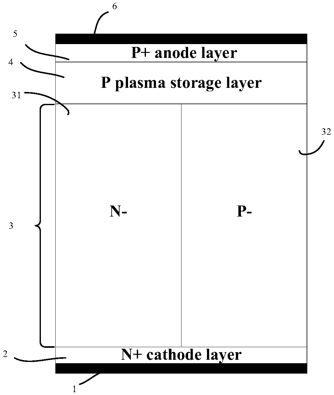
[0014] Such as figure 2 As shown, the drift step recovery diode of the present invention has a cell structure including N-type ohmic contact electrode 1, N-type heavily doped cathode region 2, super-junction withstand voltage base region 3, and P-type plasma from bottom to top. Storage layer 4, P-type heavily doped anode 5, P-type ohmic contact electrode 6; the super junction withstand voltage base region 3 includes N-column region 31 and P-column region 32; it is characterized in that, compared to the conventional p + -p-n 0 -n + For the drift step recovery diode, the withstand voltage base region of the drift step recovery diode of the present invention adopts a super junction structure.

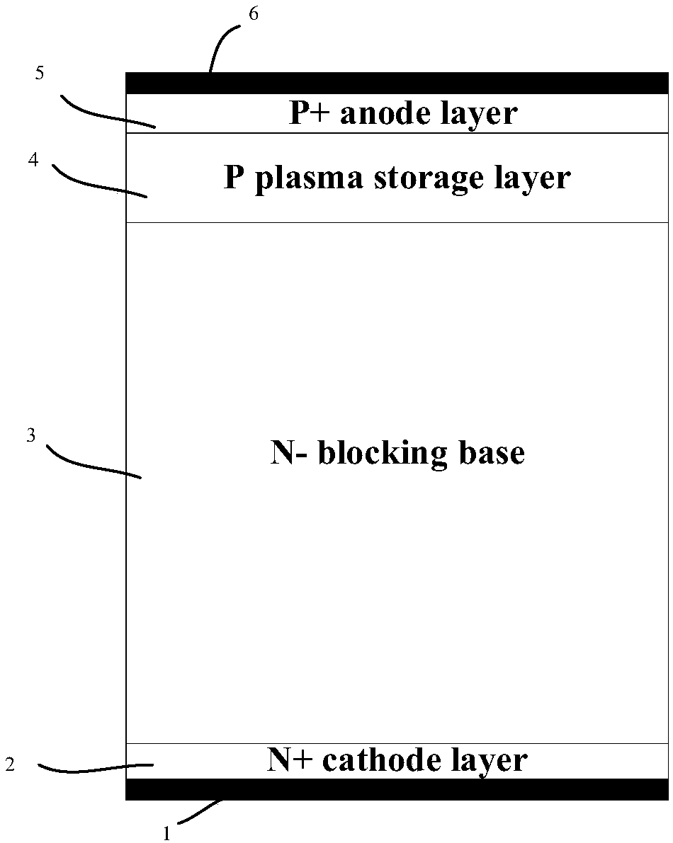
[0015] Such as figure 1 shown, for the conventional p + -p-n 0 -n + drift step recovery diode. Such as figure 2 Shown is the drift step recovery diode of the present invention. ...


PUM


Abstract

The present invention relates to power semiconductor technology, in particular to a drift step recovery diode. The withstand voltage base of a conventional p +-P-n0-n+ drift step recovery diode is modified, By changing the homogeneously doped n0 base region into a superjunction structure, that is, the superjunction withstand voltage base region 3, the carrier extraction path of the drift step recovery diode in the reverse pumping stage of the pulse discharge is changed, thereby enabling carrier extraction in both vertical and horizontal directions. The average moving distance of the minority carriers is greatly reduced, and the speed of the minority carriers extraction is accelerated, so that the time of the reverse pumping stage is reduced, and the voltage change rate of the front of thevoltage pulse formed on the load in the pulse discharge circuit is larger and the time is shorter. The superjunction base structure of the present invention uses a conventional superjunction process and does not require additional development of a new process method.

Description

technical field [0001] The invention relates to a semiconductor switch diode, in particular to a drift step recovery diode. Background technique [0002] Drift step recovery diodes (DSRD for short) is a semiconductor switching diode proposed by the Ioffe Institute of Physics and Technology in Russia. It is generally used in Ultra Wide Band (UWB) systems. Used as a key device in the signal source, it can achieve nanosecond or even picosecond switching time, and has the characteristics of high peak power, high pulse repetition frequency and high time stability. [0003] DSRD devices generally have the following technical routes, respectively p + -n 0 -n + Type DSRD devices, p + -p 0 -n + type DSRD devices as well as p + -p-n 0 -n + type DSRD devices. p + -p-n 0 -n + The type DSRD device is a commonly used scheme at the current stage. The basic working process of its pulse generating circuit has two stages: forward pumping stage and reverse pumping stage. When the...

Claims


Application Information

Patent Timeline
Patent Type & Authority Applications(China)
IPC IPC(8): H01L29/868H01L29/06
CPCH01L29/0634H01L29/868
Inventor 陈万军高吴昊邓操谯彬左慧玲夏云刘超
Owner UNIV OF ELECTRONICS SCI & TECH OF CHINA
Why Eureka
Try Eureka