
A Process Compatible Method for Monolithically Integrated Inertial Devices

A technology that integrates inertia and devices. It is used in metal material coating processes, processes for producing decorative surface effects, decorative arts, etc. It can solve the problems of large difference in structural thickness and damage of off-plane moving devices and in-plane moving devices. , to achieve the effect of reducing process deviation and improving device performance

Active Publication Date: 2021-04-30
PEKING UNIV
View PDF8 Cites 0 Cited by
  • Summary
  • Abstract
  • Description
  • Claims
  • Application Information

AI Technical Summary

Problems solved by technology

Using the traditional process will lead to a large difference in the structure thickness of the out-of-plane moving device and the in-plane moving device, and the difference in the release time of the structure will cause the structure etched first to be damaged due to over-etching

Method used


Image

  • A Process Compatible Method for Monolithically Integrated Inertial Devices
  • A Process Compatible Method for Monolithically Integrated Inertial Devices
  • A Process Compatible Method for Monolithically Integrated Inertial Devices

Examples


Embodiment Construction

[0018] The technical solutions of the present invention will be described in detail below, but the protection scope of the present invention is not limited to the embodiments.

[0019] See attached Figures 1 to 8 As shown, the above-mentioned single-chip integrated inertial device process compatibility method can adopt a process, which includes the following steps:

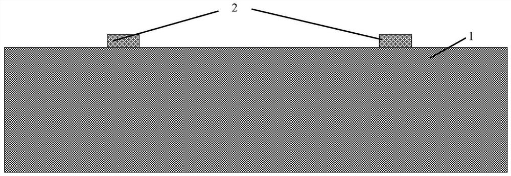
[0020] (1) grow on (111) silicon wafer 1 Silicon oxide, after photolithography, etched by RIE to form the bonding area mask 2, such as figure 1 shown;

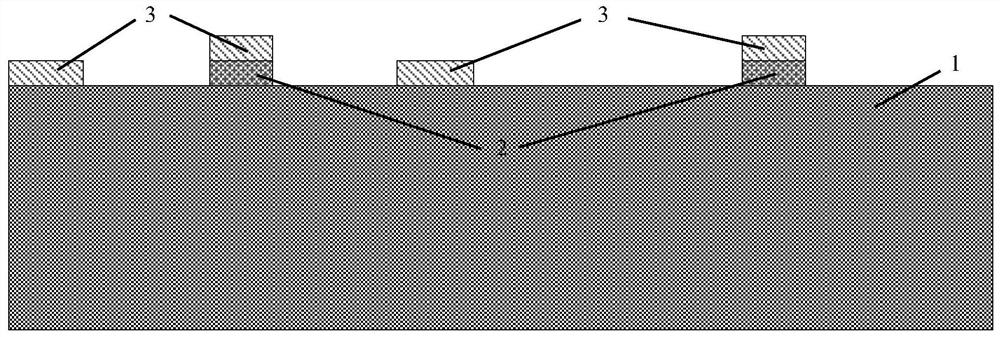
[0021] (2) Use the photoresist as a mask to carry out the second photolithography to form the mask pattern required for the steps of the back cavity with different heights. At this time, a silicon oxide mask 2 and a photoresist mask 3 are formed on the silicon wafer Composed of composite masks, such as figure 2 shown;

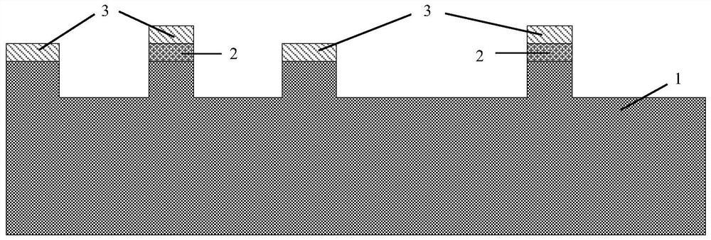
[0022] (3) Use the photoresist as a mask to perform DRIE deep etching with a depth of about 15um, such as image 3 shown;

[0023] (4) R...


PUM


Abstract

A monolithic integrated inertial device process compatible method, the process compatible method is used for a monolithic multi-axis integrated inertial device including an out-of-plane motion device and an in-plane motion device, the out-of-plane motion device includes an out-of-plane detection part and other parts, and It is characterized in that multiple back cavities and steps of different heights are formed on the back of the body by multiple etchings during processing, and the structural layer thickness of the off-plane detection part of the out-of-plane motion device is different from that of other parts of the off-plane motion device Different, the thickness of other parts of the structure layer of the out-of-plane motion device is the same as that of the in-plane motion device. When the structure is released during the process, other parts of the structural layer of the out-of-plane moving device and the structural layer of the in-plane moving device are etched through at the same time.

Description

technical field [0001] The invention relates to the field of miniature inertial measurement units (MIMUs), in particular to a process compatible method for monolithic integrated inertial devices. Background technique [0002] MEMS inertial sensor is a miniature sensor that detects and measures acceleration, tilt, shock, rotation and multi-degree-of-freedom motion. It is an important component to solve navigation, orientation and motion carrier control. A Miniature Inertial Measurement Unit (MIMU) consisting of a single, dual or triaxial accelerometer and gyroscope. MIMU can measure the acceleration and angular velocity of multiple axes of the object at the same time. After a series of data processing, the speed, displacement, direction, attitude and other information of the object can be obtained. [0003] MEMS inertial sensors have the advantages of small size, light weight, low cost, and low power consumption. They have urgent application requirements and broad applicatio...

Claims


Application Information

Patent Timeline
Patent Type & Authority Patents(China)
IPC IPC(8): B81C1/00
CPCB81C1/00531B81C1/00563B81C2201/0132
Inventor 赵前程李美杰闫桂珍
Owner PEKING UNIV
Learn More