Banknote processing device and banknote processing method
A banknote processing device and banknote processing technology, applied to coin receiving devices, thin material processing, stacking receiving devices, etc., can solve the problems of low efficiency and complicated control of banknote loading and processing, and achieve high loading processing efficiency and simple control Effect
- Summary
- Abstract
- Description
- Claims
- Application Information
AI Technical Summary
Problems solved by technology
Method used
Image
Examples
Embodiment 1
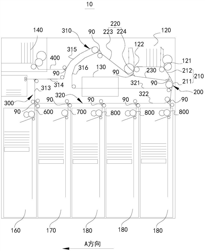
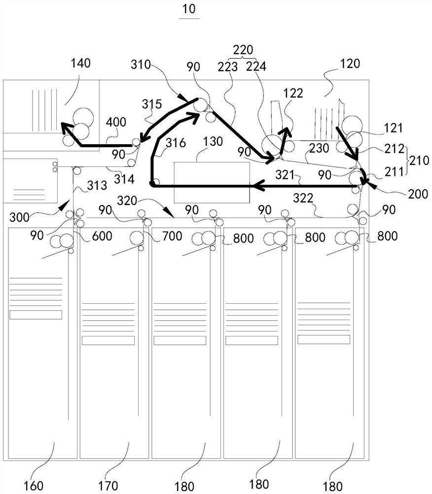
[0054] Please refer to figure 2 , figure 2 A schematic structural diagram of the banknote processing device 10 provided in this embodiment. from figure 2 As can be seen in the figure, the banknote processing device 10 includes an access mechanism 120, an identification mechanism 130, a temporary storage mechanism 140, a filling box 160, a recovery box 170, a recycling box 180, a main channel 300, an access channel 200, a temporary storage channel 400, and a filling channel. 600, recovery channel 700 and circulation channel 800.
[0055] Wherein, the access mechanism 120 is located at the top of the banknote processing device 10, and is used for users to put or take banknotes. The input and output mechanism 120 includes a currency inlet 121 for inputting banknotes and a currency output port 122 for outputting banknotes; identification mechanism 130 For identifying banknotes, the identification mechanism 130 can identify the denomination, currency, authenticity, and status...
Embodiment 2
[0098] This embodiment provides a banknote processing device 20 , which is substantially the same as the banknote processing device 10 in Embodiment 1. The difference between the two is that the banknote processing device 20 of this embodiment further includes a forgetting box 150 .
[0099] Please refer to Figure 9 , Figure 9 A schematic structural diagram of the banknote processing device 20 provided in this embodiment. from Figure 9 It can be seen that the forget box 150 is connected with the main channel 300 through the forget channel 500 . In this embodiment of the present invention, the forgetting channel 500 is connected to the first main channel 310; on the first main channel 310, the connection point between the forgetting channel 500 and the first main channel 310 is located between the filling channel 600 and the first main channel 310 between the connection point and the second end of the first main channel 310 . Further, the connection point of the forgetti...
PUM
 Abstract
Description
Claims
Application Information
 - R&D Engineer
- R&D Manager
- IP Professional
- Industry Leading Data Capabilities
- Powerful AI technology
- Patent DNA Extraction
Browse by: Latest US Patents, China's latest patents, Technical Efficacy Thesaurus, Application Domain, Technology Topic, Popular Technical Reports.
© 2024 PatSnap. All rights reserved.Legal|Privacy policy|Modern Slavery Act Transparency Statement|Sitemap|About US| Contact US: help@patsnap.com


