
Image display buffer method and device

A buffer method and buffer device technology, applied to static indicators, cathode ray tube indicators, instruments, etc., can solve the problems of high SOC cost and bandwidth consumption, and achieve the effect of avoiding bandwidth consumption and reducing costs

Active Publication Date: 2020-10-09
BEIJING VIMICRO ARTIFICIAL INTELLIGENCE CHIP TECH CO LTD
View PDF11 Cites 0 Cited by
  • Summary
  • Abstract
  • Description
  • Claims
  • Application Information

AI Technical Summary

Problems solved by technology

[0008] In view of this, the present invention is committed to providing an image display buffer method and device to simultaneously solve the problems of bandwidth consumption and high SOC cost caused by off-chip DDR in the process of display buffering

Method used


Image

  • Image display buffer method and device
  • Image display buffer method and device
  • Image display buffer method and device

Examples


Embodiment Construction

[0021] The technical solutions in the embodiments of the present invention will be clearly and completely described below in conjunction with the accompanying drawings in the embodiments of the present invention. Obviously, the described embodiments are only a part of the embodiments of the present invention, not all the embodiments. Based on the embodiments of the present invention, all other embodiments obtained by those of ordinary skill in the art without creative work shall fall within the protection scope of the present invention.

[0022] First, the following concepts are given.

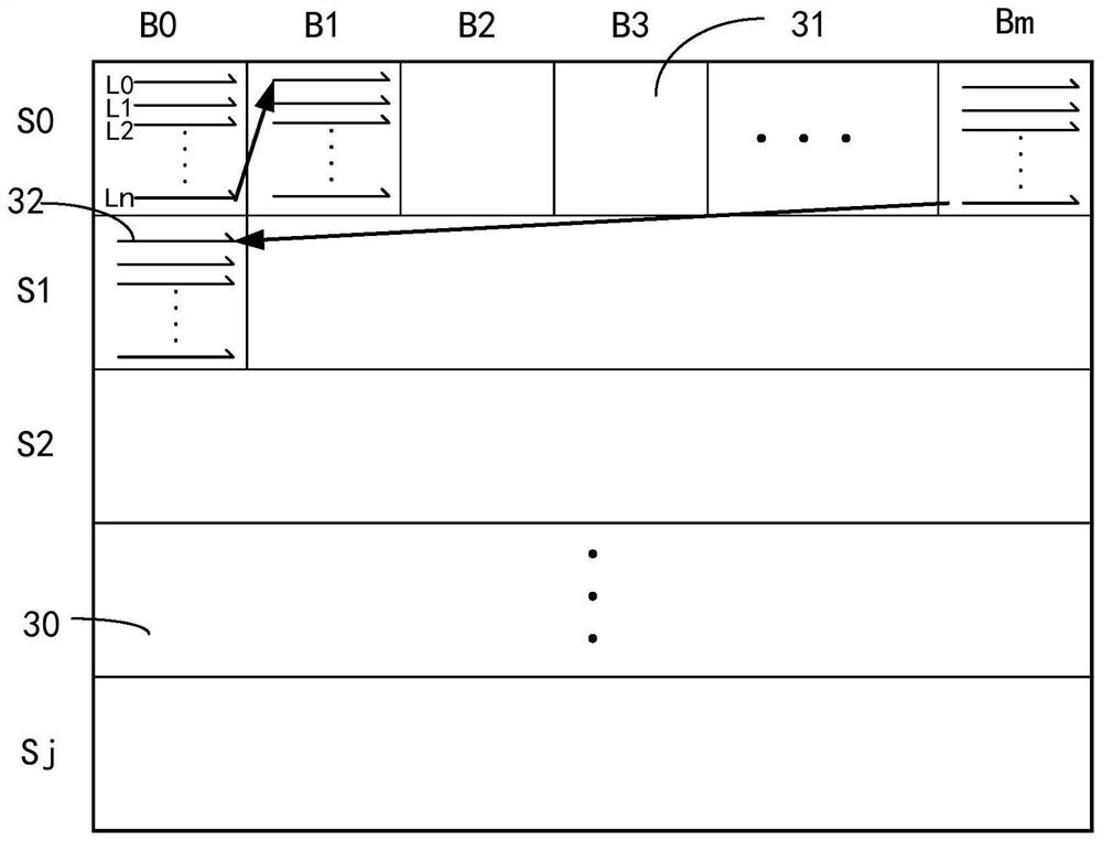
[0023] Data block refers to a block-shaped area composed of several adjacent pixels in a frame of image. Data block is the basic unit of the image compression process and is used for data transmission between memory and input and output devices. Each row of pixels in the data block is called a data row.

[0024] A stripe refers to a horizontal striped interval composed of any row of data blocks in a...


PUM


Abstract

The invention provides a display buffer method and device for an image. The problems of bandwidth consumption of an off-chip DDR and high SOC cost in the display buffer process can be solved at the same time. The display buffer method for the image comprises the steps that according to a preset address generation method, m*n read-write addresses corresponding to m*n data rows in each band among one or more bands are generated; the m*n data rows are written into storage units which the m*n read-write addresses point to according to a predetermined sequence, and the m*n read-write addresses areused as indexes for reading the m*n data rows in the m*n storage units according to scanning rows of each band among one or more bands.

Description

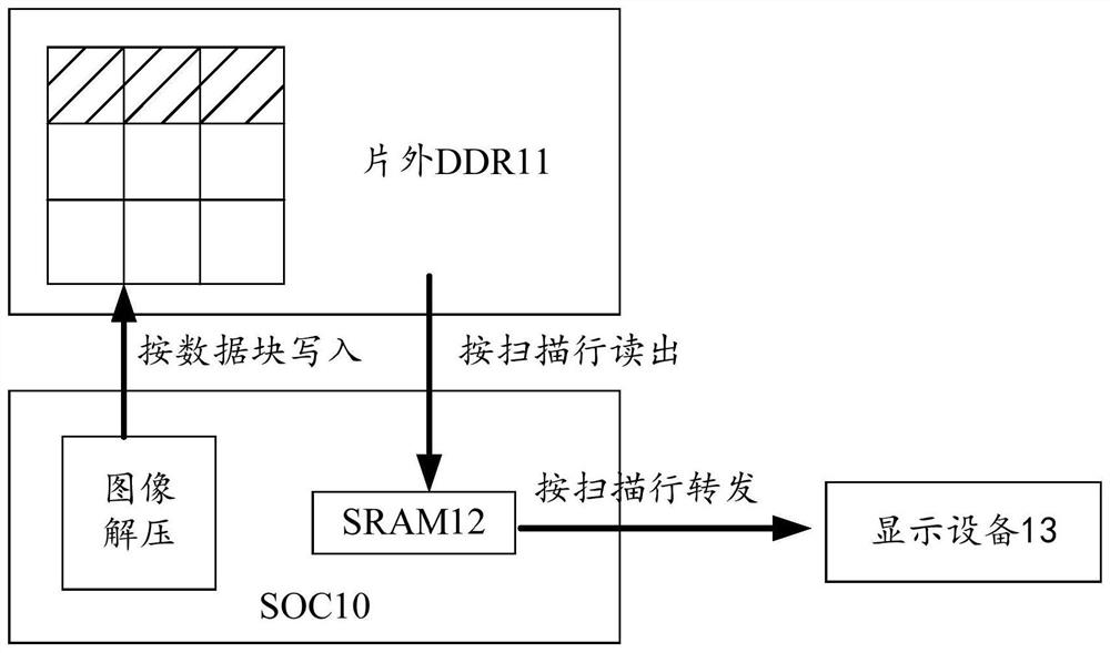
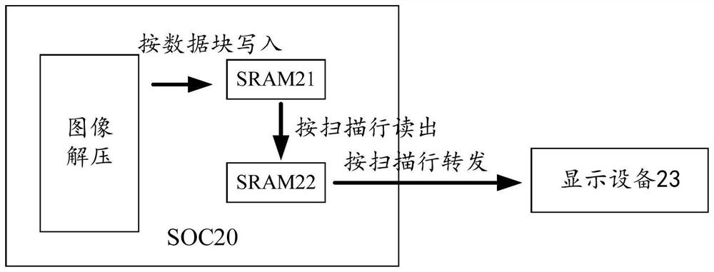
Technical field [0001] The invention relates to the technical field of image display buffering, in particular to an image display buffering method and image display buffering device. Background technique [0002] In SOC (System on Chip), it is usually necessary to output the image data stored in the SOC memory to an external display device. However, since the image data stored in the SOC memory is a compressed data block, the display device is generally All of them scan and display a frame of image line by line. Therefore, it is necessary to convert the image data stored in the memory according to the data block into scan lines. This process is called image display buffering. [0003] figure 1 Shown is a schematic diagram of a display buffering process in the prior art. From figure 1 It can be seen that the display buffering process includes: SOC10 decompresses the compressed image in the memory according to data blocks through internal operations, and then writes the decompressed...

Claims


Application Information

Patent Timeline
Patent Type & Authority Patents(China)
IPC IPC(8): G09G5/36
CPCG09G5/36
Inventor 黎明夏昌盛张韵东
Owner BEIJING VIMICRO ARTIFICIAL INTELLIGENCE CHIP TECH CO LTD
Learn More