Display panel and method of making the same
A display panel and substrate technology, applied in the direction of instruments, nonlinear optics, optics, etc., can solve the problems of uneven display, inability to recover quickly, crosstalk of display panel signals, etc., and achieve the effect of suppressing coupling phenomenon and improving voltage stability
- Summary
- Abstract
- Description
- Claims
- Application Information
AI Technical Summary
Problems solved by technology
Method used
Image
Examples
Embodiment Construction
[0045] The application will be further described in detail below with reference to the drawings and embodiments. It can be understood that the specific embodiments described here are only used to explain the application, but not to limit the application. In addition, it should be noted that, for ease of description, the drawings only show a part of the structure related to the present application instead of all of the structure.
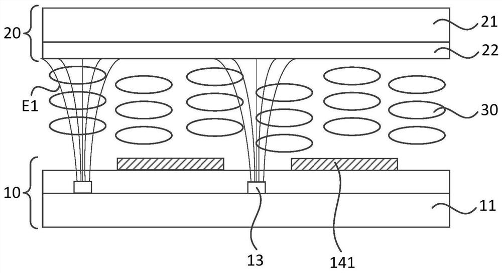
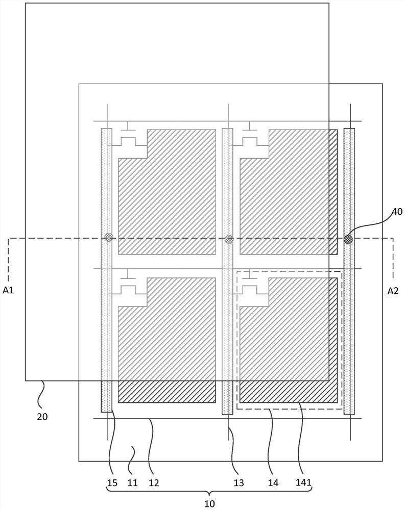
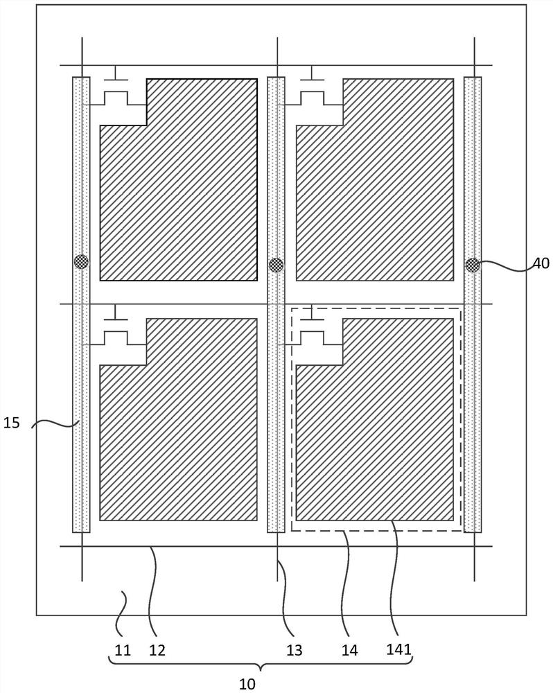
[0046] figure 1 It is a schematic diagram of the structure of an existing display panel. See figure 1 The display panel includes a first substrate 10, a second substrate 20 opposite to the first substrate 10, and a liquid crystal layer 30 located between the first substrate 10 and the second substrate 20. The first substrate 10 includes a first base substrate 11, and scan lines ( figure 1 Not shown in), the data line 13, and a plurality of pixel units defined by the intersection of the scan line and the data line 13 ( figure 1 (Not shown in); a plurali...
PUM
 Abstract
Description
Claims
Application Information
 - R&D
- Intellectual Property
- Life Sciences
- Materials
- Tech Scout
- Unparalleled Data Quality
- Higher Quality Content
- 60% Fewer Hallucinations
Browse by: Latest US Patents, China's latest patents, Technical Efficacy Thesaurus, Application Domain, Technology Topic, Popular Technical Reports.
© 2025 PatSnap. All rights reserved.Legal|Privacy policy|Modern Slavery Act Transparency Statement|Sitemap|About US| Contact US: help@patsnap.com


