Mobile phone circuit board design method, mobile phone circuit board and mobile phone
A design method and circuit board technology, applied to the structure of telephones, etc., can solve problems affecting user experience and high temperature on the side of the mobile phone
- Summary
- Abstract
- Description
- Claims
- Application Information
AI Technical Summary
Problems solved by technology
Method used
Image
Examples
no. 1 example
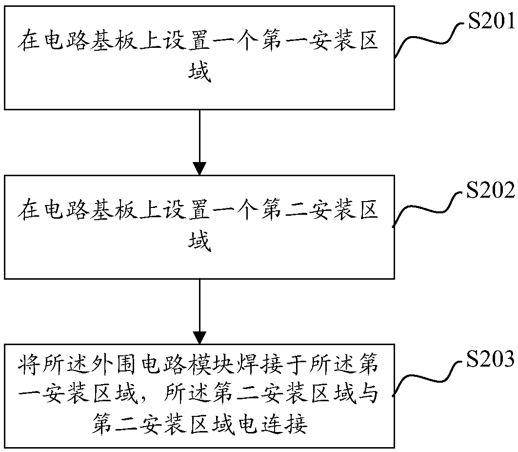
[0063] figure 2 The basic flowchart of the mobile phone circuit board design method provided in this embodiment, the mobile phone circuit board includes a circuit substrate, a peripheral circuit module and a main control module, and the peripheral circuit module and the main control module are arranged on the circuit substrate. And the mutual communication is realized through the wires on the circuit substrate. The mobile phone circuit board design method includes:
[0064] S201. Set a first installation area on a circuit substrate.
[0065] Wherein, the first installation area is mainly used for peripheral circuit modules, and the peripheral circuit modules refer to circuits or components that generate the least heat or even no heat in the mobile phone circuit, and specifically include the following circuits or devices: radio frequency Circuits, auxiliary components, audio input and output circuits, etc., these circuits are all soldered on the first installation area set a...
no. 2 example
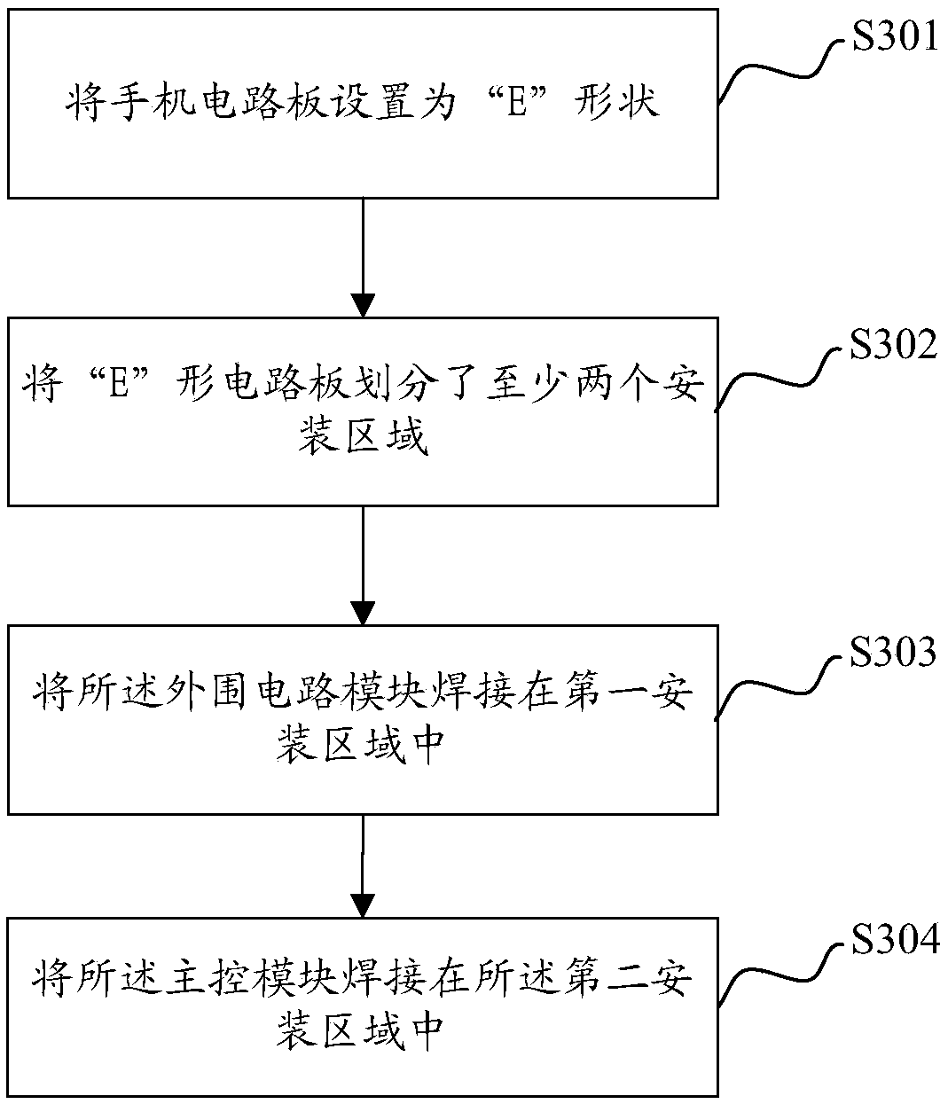
[0079] image 3 The detailed flowchart of the mobile phone circuit board design method provided by the second embodiment of the present invention. In this embodiment, the method of this embodiment will be described in detail below by taking the design of an "E" mobile phone circuit board as an example. The mobile phone circuit board Design methods include:
[0080] S301. Set the circuit board of the mobile phone into an "E" shape.
[0081] S302. Divide the "E"-shaped circuit board into at least two installation areas.
[0082] Wherein, the at least two installation areas include at least one first installation area for welding peripheral circuit modules and at least one second installation area for installing the main control module, and the first installation area must be set in The edge position of the "E"-shaped circuit board, that is, the "[" structure in "E", and the second installation area is set on the middle raised area of the "E"-shaped circuit board.
[0083] S...
no. 3 example
[0091] Please refer to Figure 4 , Figure 4 It is a structural schematic diagram of a mobile phone circuit board provided by the third embodiment of the present invention. The mobile phone circuit board 4 includes: a circuit substrate 41, a peripheral circuit module 42 and a main control module 43, and the peripheral circuit module 42 and the main control module 43 is set on the circuit substrate 41, and realizes communication through the circuit lines on the circuit substrate 41, wherein:
[0092] The circuit substrate 41 includes a first installation area 411 and a second installation area 412, the first installation area 411 is used to install the peripheral circuit module 42, and the second installation area 412 is used to install the main control module 43, and when setting the second installation area 412, specifically, the second installation area 412 is set under the first installation area 411, and the distance between the second installation area 412 and the edge o...
PUM
 Abstract
Description
Claims
Application Information
 - R&D Engineer
- R&D Manager
- IP Professional
- Industry Leading Data Capabilities
- Powerful AI technology
- Patent DNA Extraction
Browse by: Latest US Patents, China's latest patents, Technical Efficacy Thesaurus, Application Domain, Technology Topic, Popular Technical Reports.
© 2024 PatSnap. All rights reserved.Legal|Privacy policy|Modern Slavery Act Transparency Statement|Sitemap|About US| Contact US: help@patsnap.com


