Boron-containing organic light emission diode device and preparation method thereof
An electroluminescent device and electroluminescent technology, which are applied in the directions of organic light-emitting devices, organic semiconductor devices, materials of organic semiconductor devices, etc., can solve the problem of low S1 state radiation transition rate, difficult and high exciton utilization rate and high fluorescence radiation efficiency. , efficiency roll-off, etc.
Active Publication Date: 2017-12-22
JIANGSU SUNERA TECH CO LTD
View PDF4 Cites 47 Cited by
- Summary
- Abstract
- Description
- Claims
- Application Information
AI Technical Summary
Problems solved by technology
[0004] Although theoretically TADF materials can achieve 100% exciton utilization, there are actually the following problems: (1) The T1 and S1 states of the designed molecules have strong CT characteristics, and the very small S1-T1 state energy gap, although it can A high T1→S1 state exciton conversion rate is achieved through the TADF process, but at the same time it leads to
Method used
View moreImage
Smart ImageViewing Examples

Examples
 PUM
 Abstract
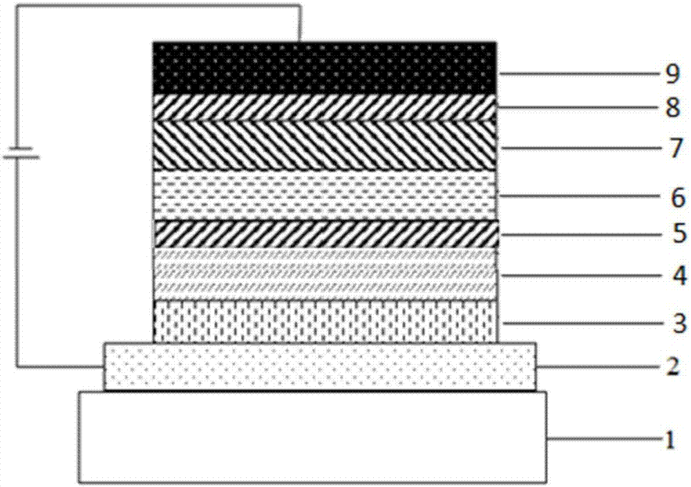
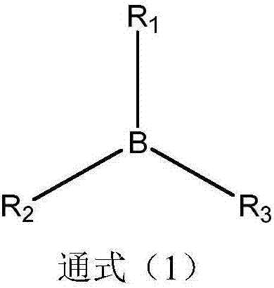
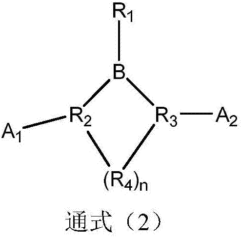
The present invention relates to an organic light emission diode device (OLED) structure, especially to a high-efficiency organic light emission diode device of a B-containing compound. The organic light emission diode device structure comprises an anode, a cavity injection/transmission layer, a luminescent layer, an electron injection/transmission layer and a cathode, wherein the luminescent layer comprises main body materials and doped materials; the main body materials are formed by signal materials and are also formed by mixing materials with different structures; and the doped materials are organic compounds containing boron, the energy level difference of the singlet state and the triplet state is not larger than 0.2ev, and the energy level of the singlet state and the energy level of the triplet state of the of the main body materials are both higher than that of the doped materials to prevent energy from passback and avoid reduction of the device luminescence efficiency. The present invention further provides a preparation method of the organic light emission diode device. The preparation method is utilized to obtain the organic light emission diode device which is high in efficiency, long in life and high in purity.
Description
technical field [0001] The invention relates to the technical field of semiconductors, in particular to the application of a boron-containing organic compound as a light-emitting layer doping material on an organic light-emitting diode and a device preparation method. Background technique [0002] Organic electroluminescent (OLED: Organic Light Emission Diodes) device technology can be used to manufacture new display products and also can be used to make new lighting products, which is expected to replace the existing liquid crystal display and fluorescent lighting, and has a wide application prospect. The OLED light-emitting device is like a sandwich structure, including electrode material film layers, and organic functional materials sandwiched between different electrode film layers. Various functional materials are superimposed on each other according to the application to form an OLED light-emitting device. As a current device, when a voltage is applied to the electrode...
Claims
Login to View More Application Information
Patent Timeline
 IPC IPC(8): H01L51/50H01L51/54
CPCH10K85/00H10K50/00H10K2102/00H10K2102/301H10K85/636H10K85/322H10K85/6574H10K85/657H10K85/6572H10K50/11H10K2101/90H10K2101/20H10K85/633H10K85/654H10K50/15H10K50/16H10K2101/10
Inventor 李崇叶中华张兆超王立春
Owner JIANGSU SUNERA TECH CO LTD
Features
- Generate Ideas
- Intellectual Property
- Life Sciences
- Materials
- Tech Scout
- Unparalleled Data Quality
- Higher Quality Content
- 60% Fewer Hallucinations
Learn More Browse by: Latest US Patents, China's latest patents, Technical Efficacy Thesaurus, Application Domain, Technology Topic, Popular Technical Reports.
© 2025 PatSnap. All rights reserved.Legal|Privacy policy|Modern Slavery Act Transparency Statement|Sitemap|About US| Contact US: help@patsnap.com