
Flickering debug method and device of liquid crystal display panel

A liquid crystal display panel and debugging method technology, applied in static indicators, nonlinear optics, optics, etc., can solve problems such as afterimages, different brightness of display screens, and affecting the normal flipping of liquid crystal molecules in liquid crystal cells

Active Publication Date: 2017-08-18
BOE TECH GRP CO LTD
View PDF6 Cites 20 Cited by
  • Summary
  • Abstract
  • Description
  • Claims
  • Application Information

AI Technical Summary

Problems solved by technology

[0003] However, due to differences in LCD manufacturing processes and the influence of impurity ions in the liquid crystal cell, the above-mentioned common voltage Vcom has a certain offset in the actual display, that is, there is an offset voltage between the actual common voltage and the theoretical common voltage △V, when the liquid crystal panel is used for display, especially for some special industries (instrument panel, long-time display instrument, map, etc.), it will seriously affect the normal flip of the liquid crystal molecules in the liquid crystal cell, which will easily lead to the When a gray-scale voltage (including positive gray-scale voltage and negative polarity gray-scale voltage) is applied to the display panel, the brightness of the display screen corresponding to the positive polarity gray-scale voltage and the negative polarity gray-scale voltage will be different, and the display screen will flicker, which will cause afterimage phenomenon

Method used


Image

  • Flickering debug method and device of liquid crystal display panel
  • Flickering debug method and device of liquid crystal display panel
  • Flickering debug method and device of liquid crystal display panel

Examples


Embodiment Construction

[0027] The following will clearly and completely describe the technical solutions in the embodiments of the present invention with reference to the accompanying drawings in the embodiments of the present invention. Obviously, the described embodiments are only some, not all, embodiments of the present invention. Based on the embodiments of the present invention, all other embodiments obtained by persons of ordinary skill in the art without making creative efforts belong to the protection scope of the present invention.

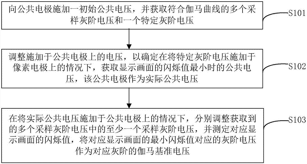
[0028] An embodiment of the present invention provides a flicker debugging method for a liquid crystal display panel. The liquid crystal display panel includes a common electrode and a pixel electrode, such as figure 2 As shown, the flashing debugging method includes:

[0029] Step S101 , applying an initial common voltage to the common electrode, and acquiring a plurality of sampled gray-scale voltages and a specific gray-scale voltage conforming to the gamm...


PUM


Abstract

The embodiment of the invention provides a flickering debug method and device of a liquid crystal display panel, pertaining to the technical field of display. By adjusting gray-scale voltage, flickering values of display images corresponding to multiple gray scales are minimized so that the possibility of flickering on display images during full gray-scale display is reduced. The flickering debug method comprises the following steps: applying initial common voltage to a common electrode and obtaining multiple sampling gray-scale voltage and one specific gray-scale voltage meeting the gamma curve; regulating voltage applied to the common electrode to determine that the common electrode when the display images are at the minimum flickering values is obtained on the condition that specific gray-scale voltage is applied to pixel electrodes; adjusting at least one sampling gray-scale voltage in obtained gray-scale voltage, measuring the flickering value of corresponding display images and taking gray-scale voltage corresponding to the minimum flicking value of corresponding display images as gamma reference voltage of corresponding gray scales.

Description

technical field [0001] The invention relates to the field of display technology, in particular to a method and device for debugging the flicker of a liquid crystal display panel. Background technique [0002] In a Liquid Crystal Display (LCD for short), the pixel voltage Vn applied to the pixel electrode varies up and down with the common voltage Vcom applied to the common electrode, as shown in figure 1 As shown, the pixel voltages V0-V255 correspond to gray scale 0 to gray scale 255, wherein, when the pixel voltage is greater than the common voltage Vcom, the pixel is positive; when the pixel voltage is lower than the common voltage Vcom, the pixel is negative. For the pixel voltage corresponding to each gray scale, the two frames before and after are greater than the common voltage Vcom and greater than the common voltage Vcom, and the absolute value of the difference between the signal voltage of the two frames before and after and the common voltage Vcom is the same, so...

Claims


Application Information

Patent Timeline
Patent Type & Authority Applications(China)
IPC IPC(8): G02F1/133G02F1/13
Inventor 张永新王世豪
Owner BOE TECH GRP CO LTD
Learn More