Graphene microstrip line traveling wave absorption optical modulator based on strip optical waveguide

An optical modulator and microstrip line technology, applied in the field of optoelectronics, can solve problems such as small modulation bandwidth, and achieve the effects of improving modulation bandwidth, improving modulation efficiency, and being easy to integrate

Active Publication Date: 2019-07-16
UNIV OF ELECTRONICS SCI & TECH OF CHINA
View PDF5 Cites 0 Cited by
  • Summary
  • Abstract
  • Description
  • Claims
  • Application Information

AI Technical Summary

Problems solved by technology

[0004] The purpose of the present invention is to solve the problem that the graphene-based optical modulator is limited by the larger RC constant of the lumped electrode structure in the prior art, resulting in a relatively small modulation bandwidth, and provides a graphene-based strip optical waveguide Microstrip Traveling Wave Absorption Optical Modulator

Method used


Image

  • Graphene microstrip line traveling wave absorption optical modulator based on strip optical waveguide
  • Graphene microstrip line traveling wave absorption optical modulator based on strip optical waveguide
  • Graphene microstrip line traveling wave absorption optical modulator based on strip optical waveguide

Examples


Embodiment Construction

[0027] In order to make the object, technical solution and advantages of the present invention clearer, the present invention will be further described in detail below in conjunction with the accompanying drawings and embodiments. It should be understood that the specific embodiments described here are only used to explain the present invention, not to limit the present invention.

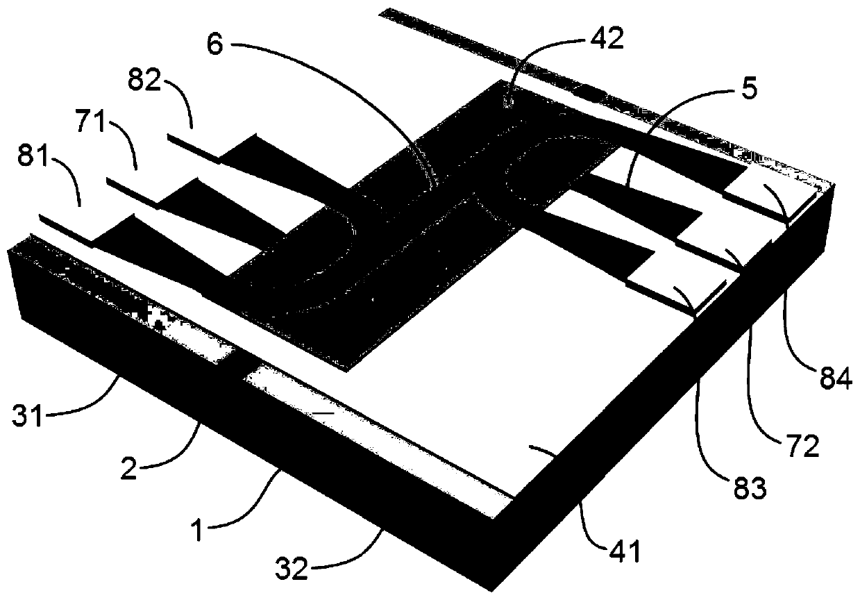
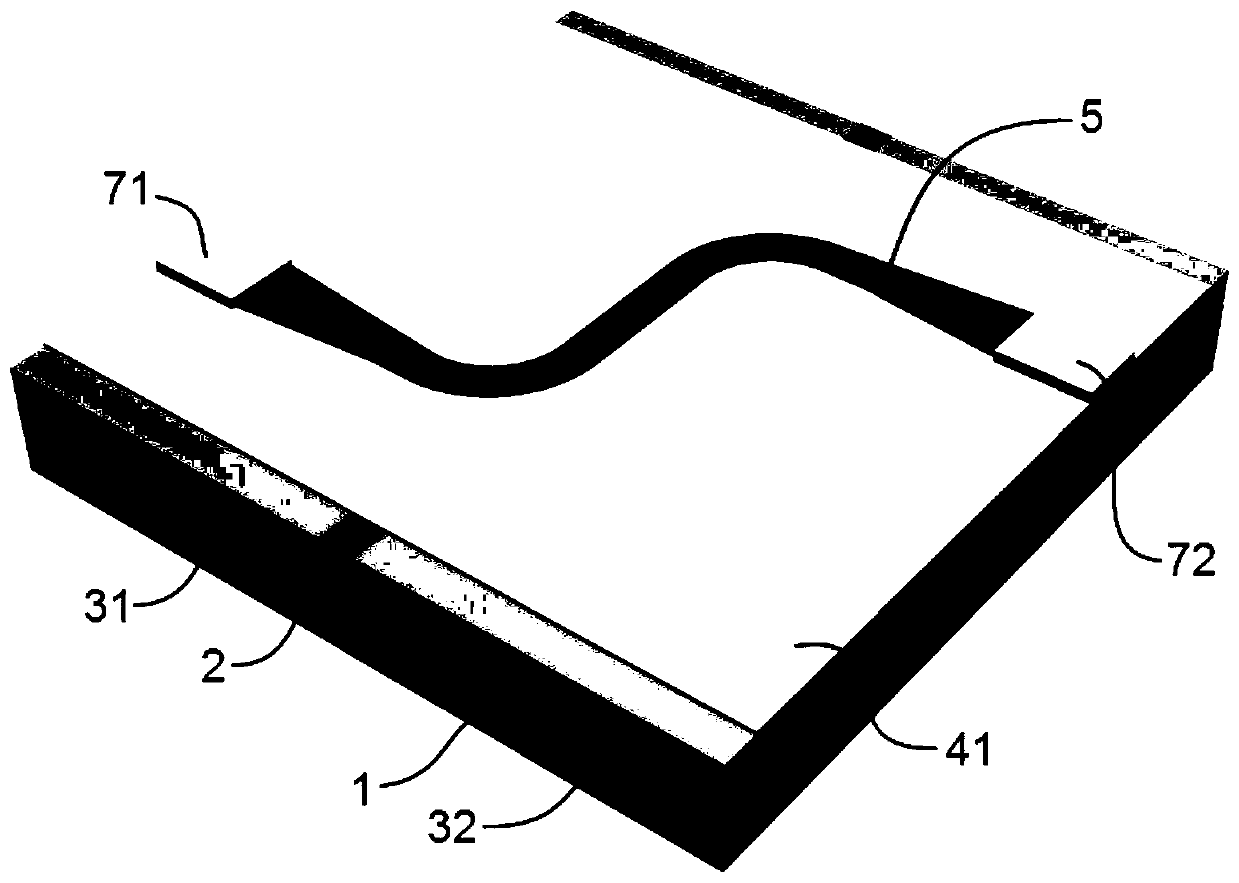
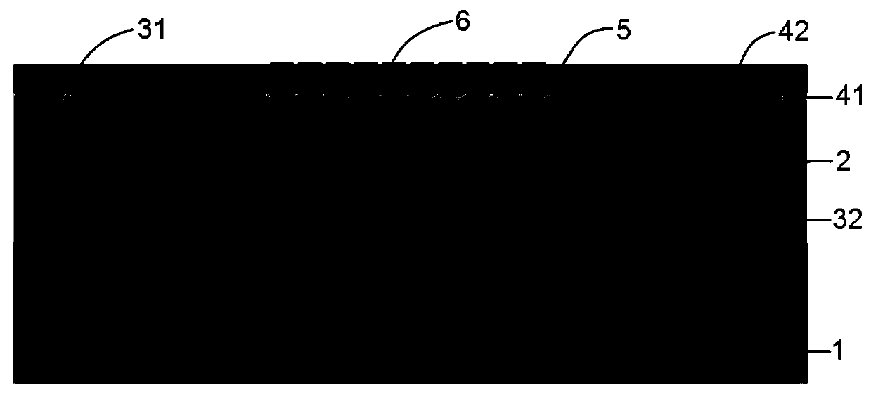
[0028] A graphene microstrip line traveling wave absorption optical modulator based on a strip optical waveguide, such as figure 1 , figure 2 and image 3 As shown, it includes a strip optical waveguide 2 arranged on a silicon dioxide substrate layer 1; the strip optical waveguide 2 divides the surface of the substrate layer 1 into two parts, the two sides of the strip optical waveguide 2, and the silicon dioxide substrate layer 1 is provided with a first dielectric filling layer 31 and a second dielectric filling layer 32; the upper surface of the strip optical waveguide 2 is sequentially provi...


PUM

PropertyMeasurementUnit
thicknessaaaaaaaaaa
thicknessaaaaaaaaaa

Abstract

The invention discloses a graphene microstrip line traveling wave absorption optical modulator based on a strip optical waveguide, which solves the problem that the graphene-based optical modulator in the prior art is limited by the large RC constant of the lumped electrode structure, which causes The problem of relatively small modulation bandwidth belongs to the field of optoelectronic technology. The invention comprises a substrate layer, a strip-shaped optical waveguide and a dielectric filling layer arranged on the surface of the substrate layer, and a microstrip traveling-wave electrode structure arranged on the strip-shaped optical waveguide. The present invention is used to achieve light modulation rate.

Description

technical field [0001] The invention discloses a graphene microstrip line traveling wave absorption optical modulator based on a strip optical waveguide, which is used to realize the optical modulation rate and belongs to the field of optoelectronic technology. Background technique [0002] With the advent of the era of big data, data communication services are growing explosively, which makes people's demand for bandwidth higher and higher, which also determines the development of optical transmission systems in the direction of ultra-high speed, large capacity, and integration. Optical modulators and optical switches are the core devices in optical communication networks, and play an important role in the construction of optical communication networks. At present, optical modulators based on various mechanisms have been developed and prepared successively, and the current commercialized modulators are mainly based on lithium niobate materials and InP-based optical modulato...

Claims


Application Information

Patent Timeline
Patent Type & Authority Patents(China)
IPC IPC(8): G02F1/035G02F1/03
CPCG02F1/0316G02F1/035
Inventor 陆荣国叶胜威刘天良夏瑞杰陈德军张尚剑刘永
Owner UNIV OF ELECTRONICS SCI & TECH OF CHINA
Why Eureka
Try Eureka