A method for manufacturing an air bridge in a semiconductor process
A manufacturing method and an air bridge technology, which are applied in semiconductor/solid-state device manufacturing, semiconductor devices, and photolithography on patterned surfaces, etc., can solve problems such as complicated process flow, erosion, and low resolution of positive photoresist, Achieve high photosensitivity and strong anti-developing effects
- Summary
- Abstract
- Description
- Claims
- Application Information
AI Technical Summary
Problems solved by technology
Method used
Image
Examples
Embodiment 1
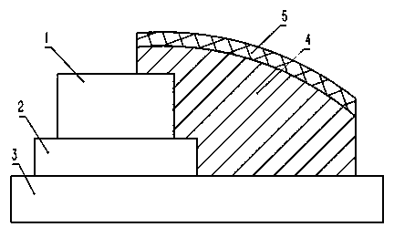
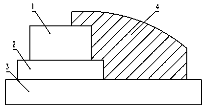
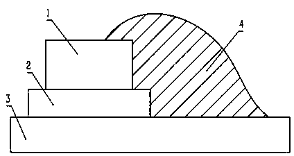
[0027] This example is mainly used to prepare air bridges on low electrode steps (such as Figure 1 As shown, "1" and "2" steps add up to less than 4um), using a single-layer LOR photoresist as the sacrificial layer, the specific preparation process is as follows:
[0028] 1) On the substrate where the electrode step etching has been completed (such as Figure 1 As shown, the sum of "1" and "2" steps is less than 4um) spin-coating a layer of LOR20A photoresist as a sacrificial layer.
[0029] 2) Spin-coat a layer of AZ52 series photoresist on the sacrificial layer as the mask layer of the sacrificial layer. After exposure and development technology, the pattern structure of the photolithography mask is transferred to the photoresist film to form the required The sacrificial layer graphic structure of ( Figure 1 shown).
[0030] 3) Exposing the substrate (that is, exposing without a photolithography mask), developing it in the developer solution for 50s, removing the upper ...
Embodiment 2
[0036] This example is mainly used to prepare air bridges on higher electrode steps (such as Figure 1 As shown, "1" and "2" steps are larger than 4um), using 2 layers of LOR photoresist as the sacrificial layer, the specific preparation process is as follows:
[0037] 1) On the substrate where the electrode step etching has been completed (such as Figure 1 As shown, two layers of LOR20A photoresist are sequentially spin-coated on the "1" and "2" steps as a sacrificial layer.
[0038] 2) Spin-coat a layer of AZ52 series photoresist on the sacrificial layer as the mask layer of the sacrificial layer. After exposure and development technology, the pattern structure of the photolithography mask is transferred to the photoresist film to form the required The sacrificial layer graphic structure of ( Figure 1 shown).
[0039] 3) Exposing the substrate (that is, exposing without a photolithography mask), developing it in the developer solution for 50s, removing the upper layer o...
PUM
 Abstract
Description
Claims
Application Information
 - Generate Ideas
- Intellectual Property
- Life Sciences
- Materials
- Tech Scout
- Unparalleled Data Quality
- Higher Quality Content
- 60% Fewer Hallucinations
Browse by: Latest US Patents, China's latest patents, Technical Efficacy Thesaurus, Application Domain, Technology Topic, Popular Technical Reports.
© 2025 PatSnap. All rights reserved.Legal|Privacy policy|Modern Slavery Act Transparency Statement|Sitemap|About US| Contact US: help@patsnap.com


